Semiconductor device and method for forming the same

a semiconductor and device technology, applied in the direction of semiconductor devices, electrical devices, transistors, etc., can solve the problems of reducing production yield, sac failure at a storage electrode contact or a bit line, sac failure at a storage electrode contact, etc., to prevent cell resistance from being increased

Inactive Publication Date: 2011-02-03
SK HYNIX INC
View PDF10 Cites 26 Cited by
  • Summary
  • Abstract
  • Description
  • Claims
  • Application Information

AI Technical Summary

Benefits of technology

[0011]Various embodiments of the present invention are directed to a method for forming a semiconductor device that substantially obviates one or more problems due to limitations and disadvantages of the related art. An object of the present invention is to provide a method for forming a semiconductor including a buried gate, such that it prevents cell resistance from being increased in inverse proportion to the size of a connection area between a contact of a storage electrode and an active region.

Problems solved by technology

In particular, a Self Align Contact (SAC) fail occurs between a landing plug and a gate or between a landing plug and a recess gate in a landing plug process, resulting in a reduced production yield.
However, the buried gate structure also has a disadvantage in that it causes the SAC fail at a storage electrode contact or a bit line.
SAC fail at a storage electrode contact occurs when the storage electrode contact is not connected to an active region.

Method used


Image

  • Semiconductor device and method for forming the same
  • Semiconductor device and method for forming the same
  • Semiconductor device and method for forming the same

Examples


Embodiment Construction

[0035]Embodiments of the present invention are described below, examples of which are illustrated in the accompanying drawings. Wherever possible, the same reference numbers will be used throughout the drawings to refer to the same or like parts.

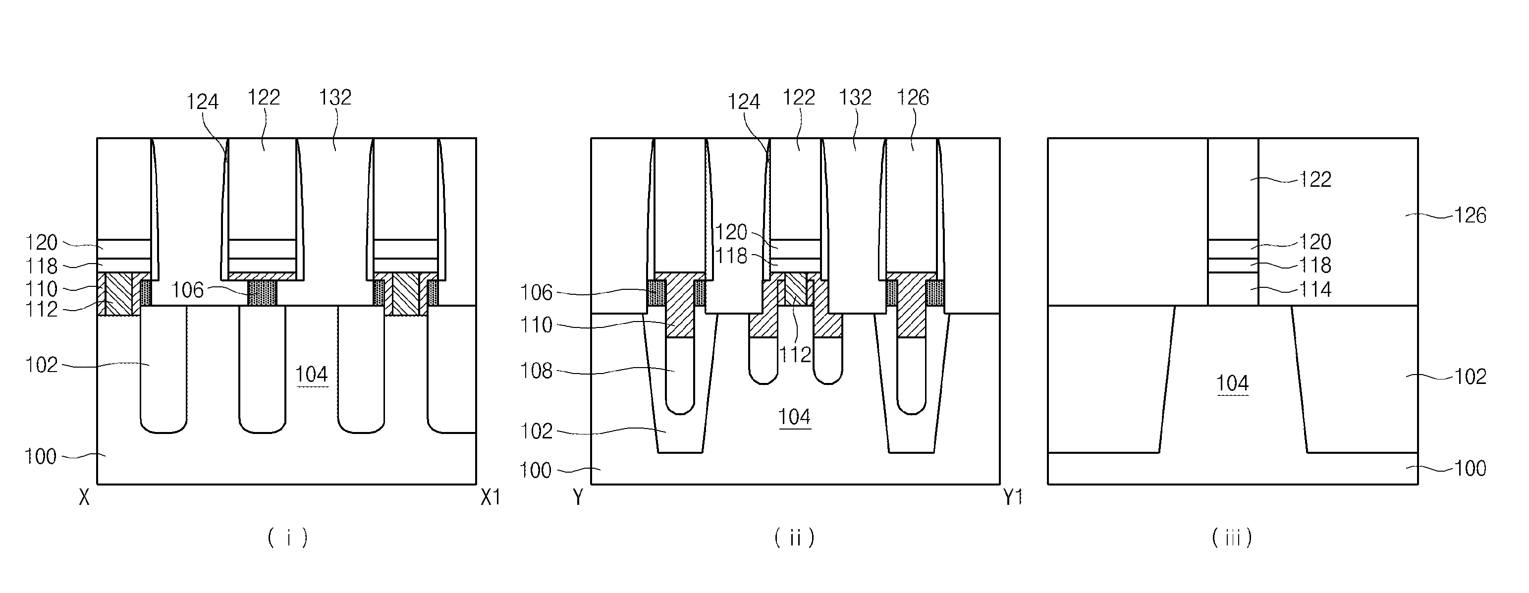
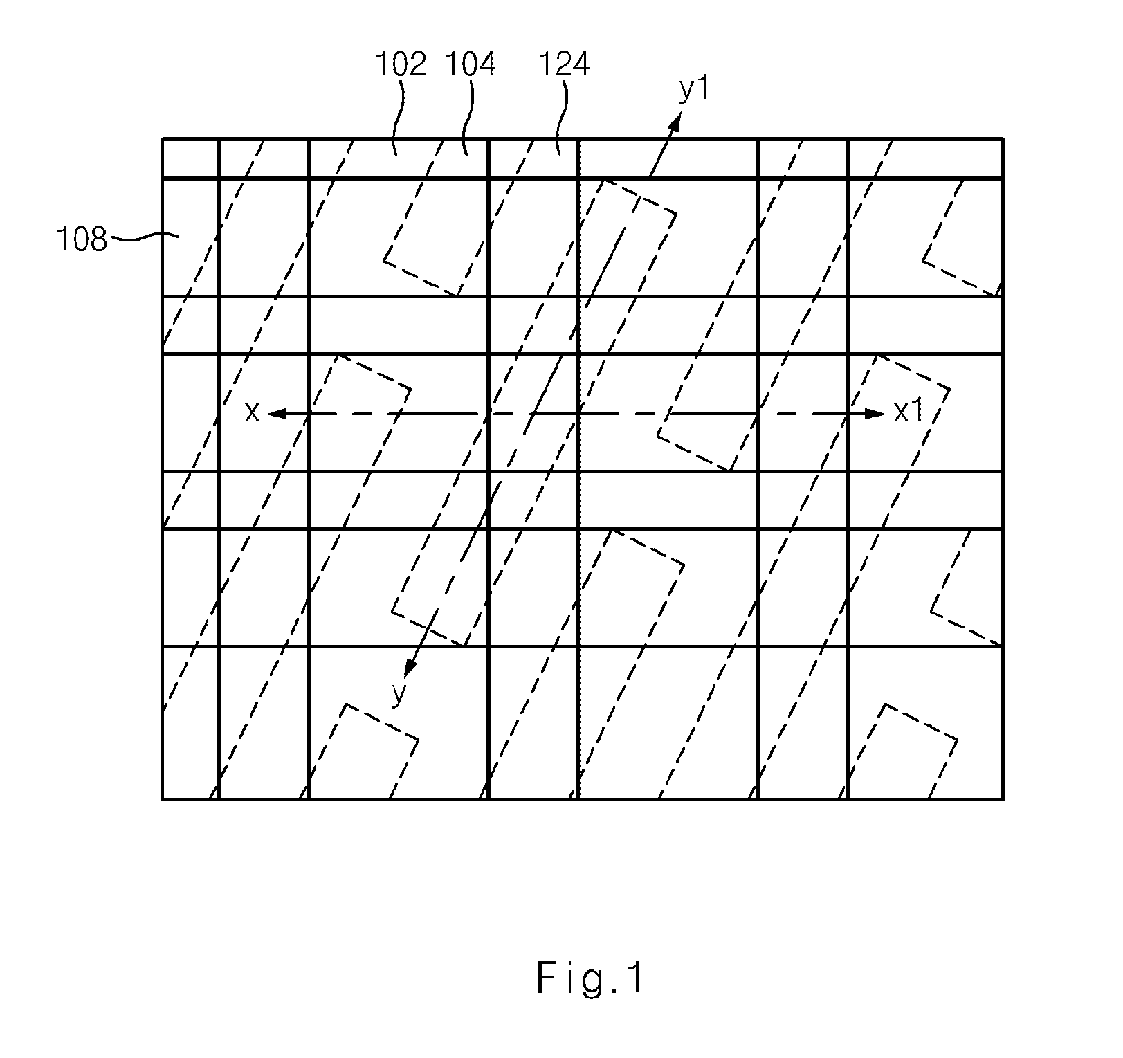
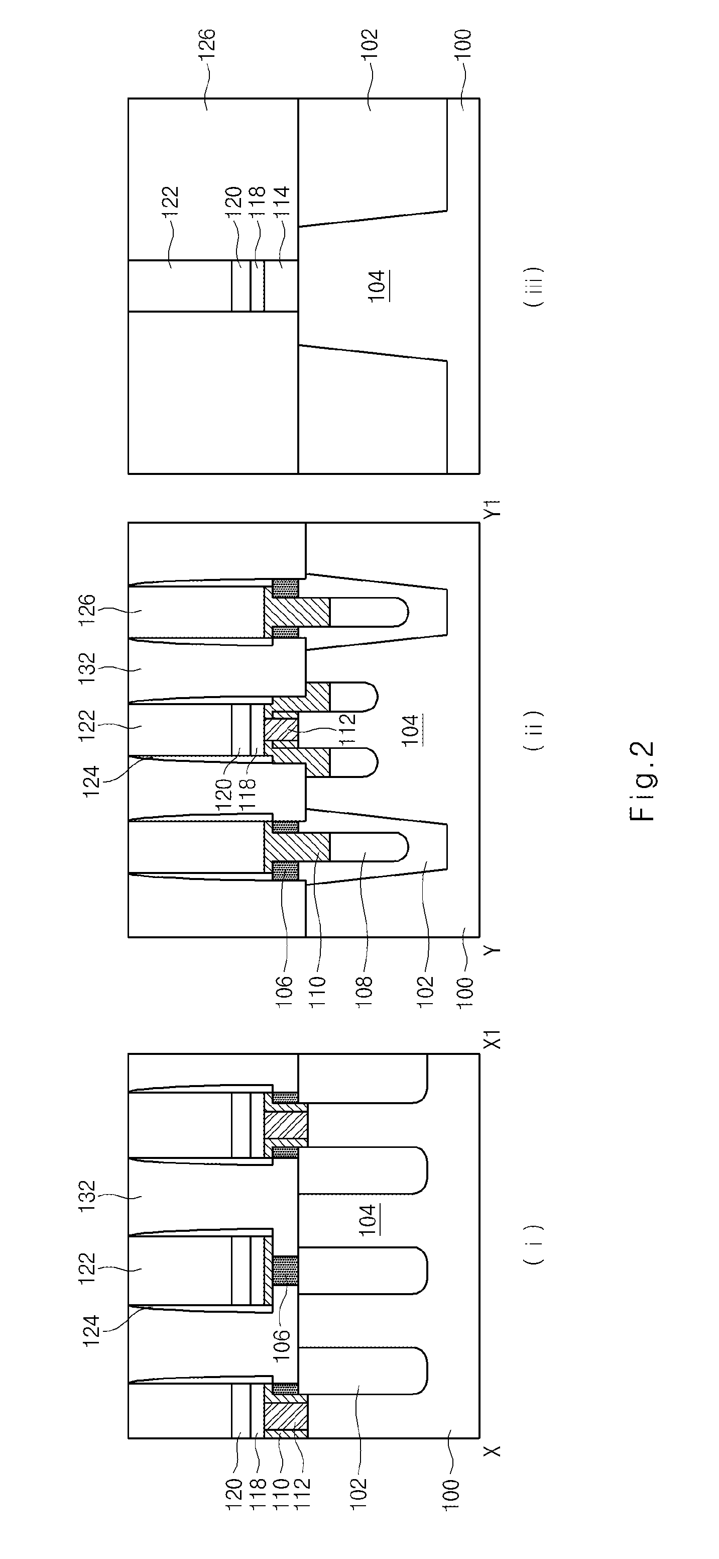
[0036]FIG. 1 is a plan view illustrating a cell area of a semiconductor device according to an embodiment of the present invention. FIGS. 2(i) to 2(iii) are cross-sectional views illustrating a semiconductor device according to the embodiment of the present invention, respectively. FIG. 2(i) is a cross-sectional view illustrating a cell area taken along the line x-x′ of FIG. 1, FIG. 2(ii) is a cross-sectional view illustrating a cell area taken along the line y-y′ of FIG. 1, and FIG. 2(iii) is a cross-sectional view illustrating a peripheral area. FIGS. 3a to 3h are cross-sectional views illustrating a method for forming a semiconductor device according to the embodiment of the present invention. Each of FIG. (i) is a cross-sectional view il...


PUM


Abstract

A method for forming a semiconductor device is disclosed. The method for forming the semiconductor device includes forming a pad insulating layer on a semiconductor substrate, forming a recess by etching the pad insulating layer and the semiconductor substrate, forming a buried gate buried in the recess, forming an insulating layer for defining a bit line contact hole over the buried gate and the pad insulating layer, forming a bit line over a bit line contact for filling the bit line contact hole, and forming a storage electrode contact hole by etching the insulating layer and the pad insulating layer to expose the semiconductor substrate. As a result, the method increases the size of an overlap area between a storage electrode contact and an active region without an additional mask process, resulting in a reduction in cell resistance.

Description

CROSS-REFERENCE TO RELATED APPLICATION[0001]The priority of Korean patent application No. 10-2009-0069068 filed on Jul. 28, 2009, the disclosure of which is hereby incorporated in its entirety by reference, is claimed.BACKGROUND OF THE INVENTION[0002]1. Field of the Invention[0003]Embodiments of the present invention relate to a method for forming a semiconductor device, and more particularly to a method for forming a semiconductor device including a buried gate.[0004]2. Background of the Invention[0005]Recently, most electronic appliances include semiconductor devices. The semiconductor devices include electronic elements, such as transistors, resistors, capacitors, and the like. These electronic elements are designed to perform functions of the electronic appliances and are integrated on a semiconductor substrate. For example, electronic appliances, such as computers, digital cameras, and the like, include semiconductor devices, such as memory chips for storage of information, pro...

Claims


Application Information

Patent Timeline
Patent Type & Authority Applications(United States)
IPC IPC(8): H01L27/06H01L21/8234
CPCH01L27/10855H01L27/10876H01L27/10885H01L29/66621H01L27/10894H01L29/4236H01L27/10888H10B12/053H10B12/485H10B12/09H10B12/0335H10B12/482H01L21/18H10B99/00H10B12/00
Inventor KIM
Owner SK HYNIX INC
Why Eureka
Try Eureka