Method and apparatus for inspecting defects in wafer

a technology of defects and wafers, applied in the direction of instruments, television systems, image enhancement, etc., can solve the problem of difficulty in extracting internal defects alone, and achieve the effect of improving work efficiency in defect inspection

Inactive Publication Date: 2011-02-03
SUMCO CORP
View PDF11 Cites 35 Cited by
  • Summary
  • Abstract
  • Description
  • Claims
  • Application Information

AI Technical Summary

Benefits of technology

[0020]According to the present invention, it is possible to simultaneously detect both internal defects and front and rear surface defects in the wafer and improve work efficiency in defect inspection.

Problems solved by technology

Thus, it is difficult to extract internal defects alone.

Method used


Image

  • Method and apparatus for inspecting defects in wafer
  • Method and apparatus for inspecting defects in wafer
  • Method and apparatus for inspecting defects in wafer

Examples


embodiment 1

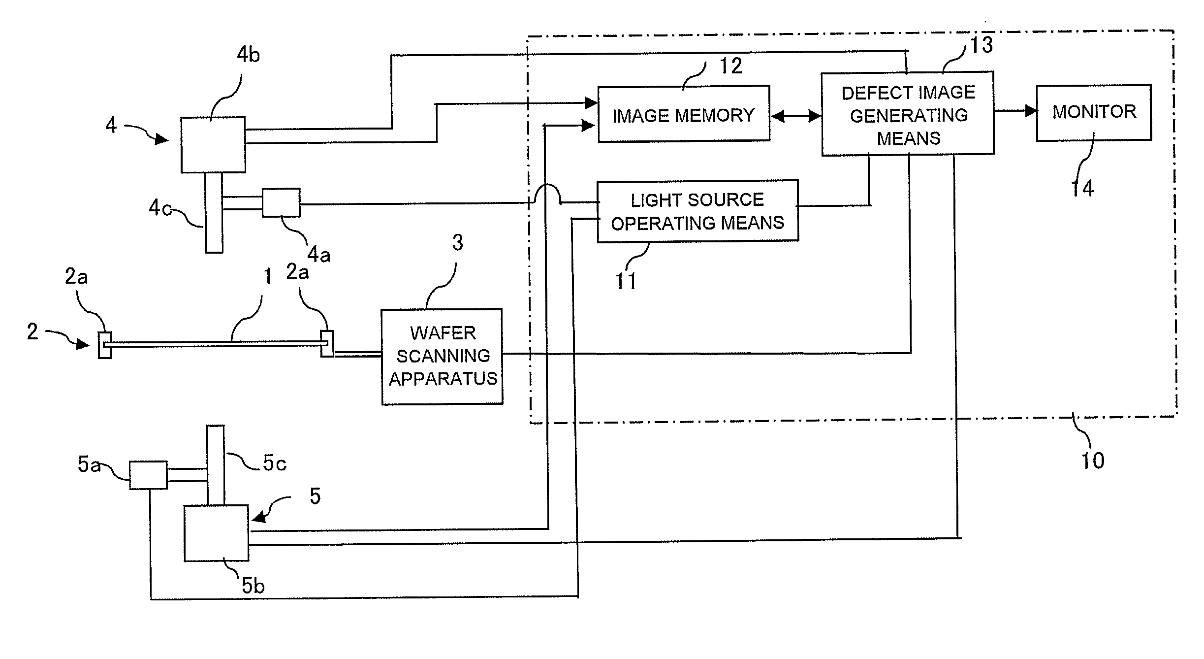
[0032]FIG. 1 shows an overall configuration diagram of a defect inspection apparatus according to embodiment 1 of the present invention. As shown in the figure, a wafer 1 under inspection is supported by an inspection bench 2 including a frame 2a for supporting plural places of a peripheral part of the wafer. In embodiment 1, the inspection bench 2 is formed so as to be movable back and forth and right and left along a surface of the wafer 1 by a wafer scanning apparatus 3. A first light source / image pickup unit 4 is arranged oppositely to one surface of the wafer (hereinafter referred to as the front surface). The first light source / image pickup unit 4 is formed by attaching a first light source 4a for irradiating infrared light and visible light while switching therebetween and a first image pickup device 4b for taking an image of the front surface to the same telecentric optical system 4c including lenses and the like. In addition, a second light source / image pickup unit 5 is arr...

embodiment 2

[0046]FIG. 4 shows a flowchart of a defect inspecting method according to embodiment 2 of the present invention. Embodiment 2 differs from embodiment 1 in that the reflected image Aij is not taken, the transmitted image Eij is taken with the amount of light made larger than when the transmitted image Bij is taken, and a defect image is generated on the basis of the reflected image Cij, transmitted image Bij and transmitted image Eij. The defect inspection apparatus is the same, except the defect image generating means 13, as that of embodiment 1, and therefore, will not be explained again.

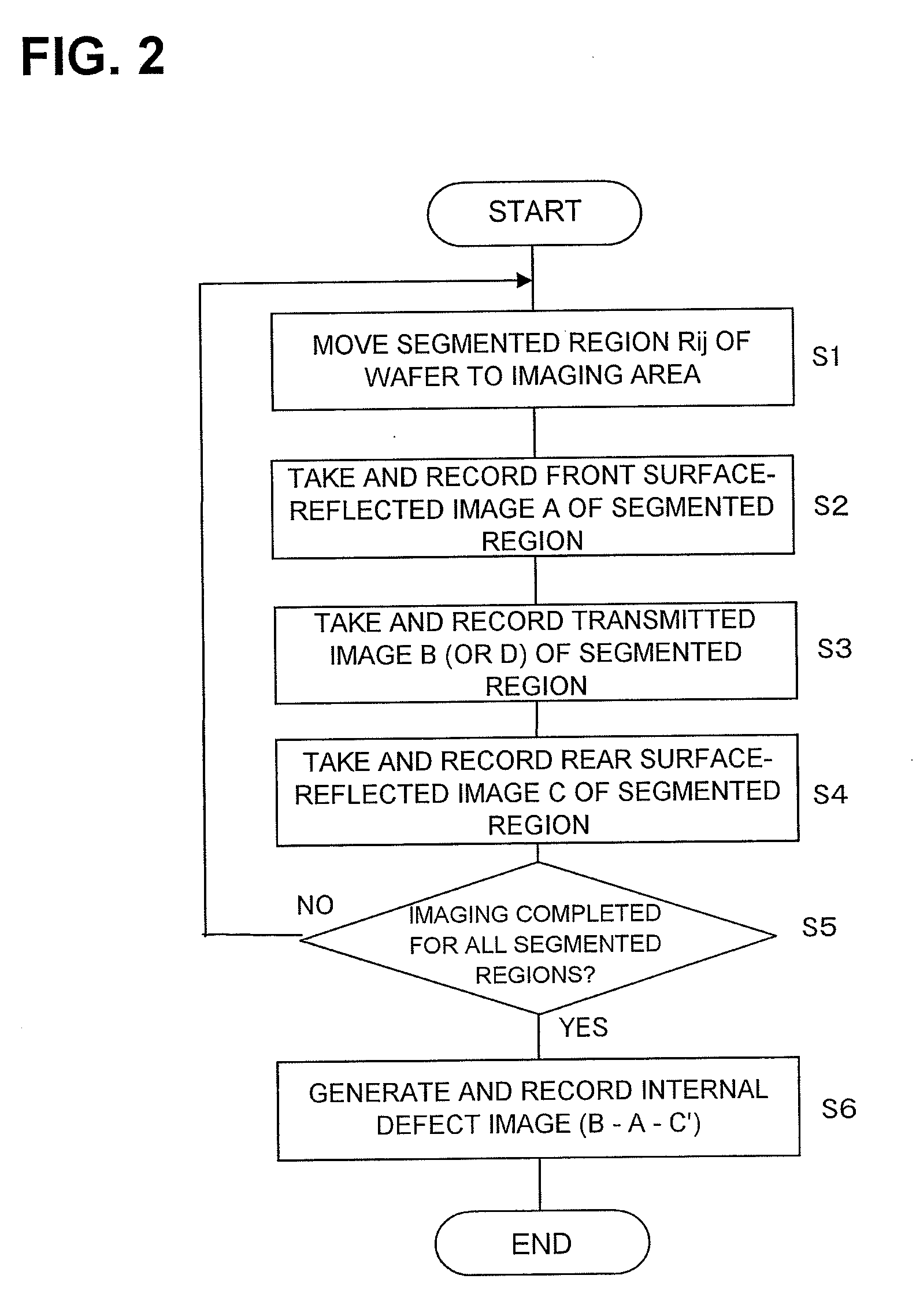
[0047]The defect image generating means 13 drives the wafer scanning apparatus 3 in accordance with the set segmented regions Rij and moves the wafer 1, so that a first segmented region R00 falls within the imaging visual field (S1). Next, the defect image generating means 13 operates the light source operating means 11 to irradiate infrared light (or visible light) from the light source 5a to the ...

embodiment 3

[0052]FIG. 7 shows an overall configuration diagram of a defect inspection apparatus according to embodiment 3 of the present invention. Embodiment 3 differs from embodiment 1 in that an image pickup unit 15 equipped with an image pickup device 4b and an optical system 4c is disposed at one surface of the wafer 1 in place of the light source / image pickup units 4 and 5, and an optical unit 16 equipped with an unillustrated light source and optical system is disposed at the other surface of the wafer 1, so that the optical axes of the image pickup unit 15 and the optical unit 16 agree with each other. Another difference is that the defect image generating means 13 includes judgment data indicative of the luminance range of pixels corresponding to an internal defect in the wafer 1. The rest of configuration is the same as that of embodiment 1, and therefore, like components are denoted by like reference characters and will not be explained again.

[0053]The principles of defect inspectio...


PUM


Abstract

An object of the present invention is to simplify the defect inspection of an internal defect and front and rear surface defects in a wafer. A defect inspection method of the present invention includes: a first imaging step of taking a transmitted image of a wafer 1 by disposing two light source/image pickup units 4 and 5 equipped with a light source, an image pickup device and an optical system oppositely to each other across the wafer 1, irradiating infrared light from at least one of the light source/image pickup units 4 and 5 to the wafer 1, and receiving transmitted light from the wafer 1; a second imaging step of taking the respective reflected images of both wafer surfaces by irradiating infrared light or visible light from the light source/image pickup units 4 and 5 to the wafer 1 and receiving reflected light from the wafer 1; and an extraction step of extracting the defects in the wafer 1 on the basis of the transmitted image and the reflected images of both surfaces, thereby simultaneously detecting both an internal defect and front and rear surface defects in the wafer.

Description

BACKGROUND OF THE INVENTION[0001]1. Field of the Invention[0002]The present invention relates to a method and an apparatus for inspecting defects in a wafer, and more particularly, to a technique for inspecting internal defects and front and rear surface defects in the wafer by using transmitted images obtained by irradiating infrared light to the wafer.[0003]2. Description of the Related Art[0004]For example, a technique for inspecting internal defects in a wafer is described in JP2006-351669A. According to this technique, infrared light is irradiated from one surface of a wafer and infrared light having transmitted through the wafer is received by an infrared camera disposed at the other surface of the wafer. Then, the wafer is inspected for internal defects on the basis of a transmitted image obtained by the transmitted infrared light. That is, if any defects, such as voids or cracks, exist within the wafer, the irradiated infrared light is scattered by the defects within the waf...

Claims


Application Information

Patent Timeline
Patent Type & Authority Applications(United States)
IPC IPC(8): H04N7/18G06K9/00
CPCG01N21/9501G01N21/9505G06T7/0004G06T2207/30148G06T2207/10152G06T2207/20224G06T2207/10048
Inventor NINOMIYA, MASAHARU
Owner SUMCO CORP
Why Eureka
Try Eureka