

Display device
a technology of a display panel and a gate line, which is applied in the direction of instruments, computing, electric digital data processing, etc., can solve the problem that the gate line cannot be arranged in the inside of the liquid crystal display panel, and achieve the effect of preventing the deterioration of reducing the stress applied to the resetting thin film transistor
- Summary
- Abstract
- Description
- Claims
- Application Information
AI Technical Summary
Benefits of technology
Problems solved by technology
Method used
Image

Examples
embodiment 1
[0052]FIG. 3 shows an equivalent circuit of a TFT-type active-matrix liquid crystal display panel according to an embodiment 1 of the present invention.
[0053]As shown in FIG. 3, a liquid crystal display panel according to this embodiment includes, on a liquid-crystal-side surface of one substrate of a pair of substrates which are arranged to face each other in an opposed manner with liquid crystal sandwiched therebetween, a plurality of scanning lines (also referred to as “gate lines”) (GL-R, GL-G, GL-B) and a plurality of video lines (also referred to as “source lines” or “drain lines”) (DL).
[0054]Regions surrounded by the scanning lines and the video lines constitute sub pixel regions, and each sub pixel region is provided with a thin film transistor (TFT) which has a gate thereof connected to the scanning line, a drain (or a source) thereof connected to the video line, and the source (or the drain) thereof connected to a pixel electrode (PX) and constitutes an active element.
[005...
embodiment 2
[0100]FIG. 7 shows an equivalent circuit of a TFT-type active-matrix liquid crystal display panel according to an embodiment 2 of the present invention.
[0101]In this embodiment, the scanning lines (GL-R, GL-G, GL-B) are driven using the three-stage constitution. In this embodiment, the scanning lines (GL-R, GL-G, GL-B) are divided into k2×k3 pieces of first groups. Each second group includes k2 pieces of first groups, and each third group includes k3 pieces of second groups.
[0102]To be more specific, in FIG. 7, the third group includes 9 pieces (k3 pieces) of second groups, the second group includes 12 pieces (k2 pieces) of first groups, and the first group includes 24 pieces (k1 pieces) of scanning lines (GL-R, GL-G, GL-B). Accordingly, in FIG. 7, the total number of scanning lines (GL-R, GL-G, GL-B) becomes 2592 (2592=24×12×9). Accordingly, the scanning circuit (RDV) includes, as terminals for the scanning lines (GL-R, GL-G, GL-B), 24 pieces (k1 pieces) of terminals belonging to t...
embodiment 3
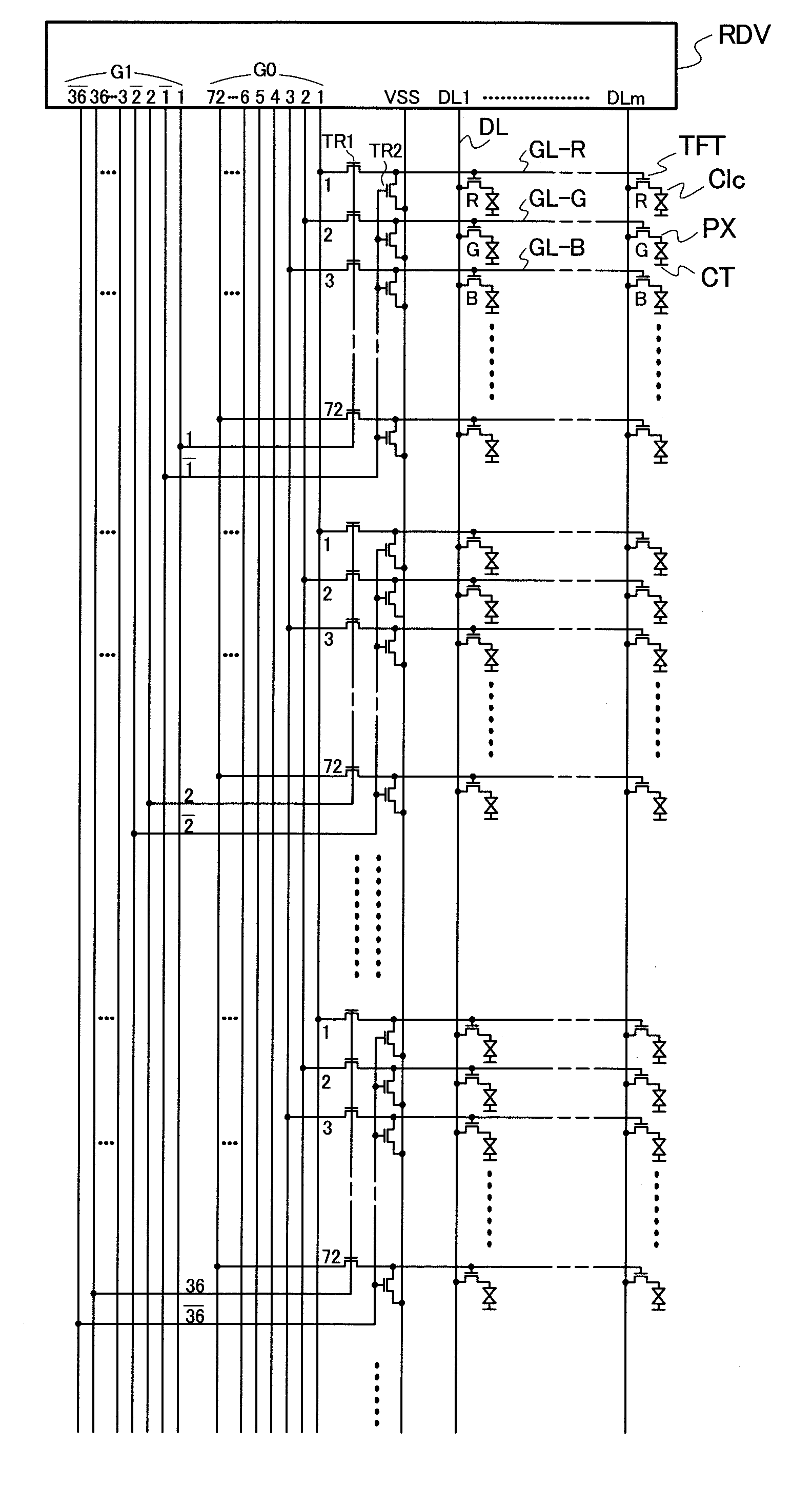
[0130]FIG. 11 shows an equivalent circuit of a TFT-type active-matrix liquid crystal display panel according to an embodiment 3 of the present invention. FIG. 12 shows an arrangement state of first transistors (TR1) and second transistors (TR2) shown in FIG. 11.
[0131]Also in this embodiment, one pixel is constituted of a sub pixel of red (R) which is first color, a sub pixel of green (G) which is second color and a sub pixel of blue (B) which is third color. However, in this embodiment, a video voltage (so-called a grayscale voltage) is inputted to the sub pixel of red (R), the sub pixel of green (G) and the sub pixel of blue (B) in one pixel via different video lines (DL).
[0132]Accordingly, in this embodiment, an RGB switch circuit (RGB-SW) is provided to a scanning circuit (RDV) side. With this RGB switch circuit (RGB-SW), video voltages of red (R), green (G) and blue (B) which are outputted from the scanning circuit (RDV) during 1H period are respectively outputted to video lines...
PUM
 Abstract
Description
Claims
Application Information