Display device and manufacturing method thereof

a technology of a display device and a manufacturing method, applied in the field of display devices, can solve the problem of requiring a wiring removal process and achieve the effect of preventing the influence of exposed wiring

Active Publication Date: 2011-02-24
PANASONIC LIQUID CRYSTAL DISPLAY CO LTD
View PDF3 Cites 0 Cited by
  • Summary
  • Abstract
  • Description
  • Claims
  • Application Information

AI Technical Summary

Benefits of technology

[0008]The present invention has an object to provide a manufacturing method for a display device, with which an influence caused by exposed wirings may be prevented without increasing the number of processes.
[0009](1) A manufacturing method for a display device according to one aspect of the present invention includes: a step (a) of forming a semiconductor layer above a substrate; a step (b) of forming a metallic layer on the semiconductor layer; a step (c) of forming, on the metallic layer, an etching resist including a first portion and a second portion, the first portion being thicker than the second portion; a step (d) of etching and patterning the semiconductor layer and the metallic layer through the etching resist so as to form a wiring from the metallic layer and leave the semiconductor layer under the wiring; a step (e) of conducting an electrical test on the wiring; a step (f) of thinning the etching resist to remove the second portion while leaving the first portion unremoved; a step (g) of performing selective etching through the first portion, which is left unremoved, so as to leave the semiconductor layer unetched, to thereby pattern the wiring to be divided into a drain electrode and a source electrode; and a step (h) of cutting the substrate, in which the step (g) of patterning the wiring includes etching the wiring to be cut at a position closer to a cutting line of the substrate with respect to the drain electrode and the source electrode, while leaving the semiconductor layer unetched. According to the present invention, the wiring is cut at the same time as an originally-defined process, and hence the influence caused by exposed wirings may be prevented without increasing the number of processes.
[0014](6) A manufacturing method for a display device according to still another aspect of the present invention includes: a step (a) of forming a wiring on a substrate, the wiring being patterned to include a drain electrode and a source electrode which are separate from each other; a step (b) of conducting an electrical test on the patterned wiring; a step (c) of forming a passivation film over the patterned wiring; a step (d) of etching the passivation film to form a through hole in the passivation film, which is used for establishing electrical connection to the patterned wiring; a step (e) of forming a metallic layer on the passivation film and inside the through hole on the patterned wiring; a step (f) of etching the metallic layer to form a pixel electrode; and a step (g) of cutting the substrate, in which: the step (d) of etching the passivation film includes forming one of a passing through hole and a notch in the passivation film at a position of the patterned wiring closer to a cutting line of the substrate with respect to the drain electrode and the source electrode, the one of the passing through hole and the notch having a size containing a width of the patterned wiring; the step (e) of forming the metallic layer includes further forming the metallic layer on a portion of the patterned wiring corresponding to the one of the passing through hole and the notch; and the step (f) of etching the metallic layer includes further etching the portion of the patterned wiring corresponding to the one of the passing through hole and the notch, to thereby cut the patterned wiring. According to the present invention, the wiring is cut at the same time as an originally-defined process, and hence the influence caused by exposed wirings may be prevented without increasing the number of processes.
[0016](8) A manufacturing method for a display device according to still another aspect of the present invention includes: a step (a) of forming a gate wiring on a substrate; a step (b) of conducting an electrical test on the gate wiring; a step (c) of forming a gate insulating film over the gate wiring; a step (d) of forming, on the gate insulating film, a patterned semiconductor layer and a patterned signal wiring on the patterned semiconductor layer; a step (e) of forming a passivation film over the patterned signal wiring; a step (f) of etching the passivation film to form a through hole in the passivation film, which is used for establishing electrical connection to the patterned signal wiring; a step (g) of forming a metallic layer over the passivation film and in the through hole on the patterned signal wiring; a step (h) of etching the metallic layer to form a pixel electrode; and a step (i) of cutting the substrate after the step (h) of forming the pixel electrode, in which: the step (f) of etching the passivation film includes forming one of a passing through hole and a notch in the passivation film and the gate insulating film at a position of the gate wiring closer to a cutting line of the substrate with respect to the semiconductor layer, the one of the passing through hole and the notch having a size containing a width of the gate wiring; the step (g) of forming the metallic layer includes further forming the metallic layer on a portion of the gate wiring corresponding to the one of the passing through hole and the notch; and the step (h) of etching the metallic layer includes further etching the portion of the gate wiring corresponding to the one of the passing through hole and the notch, to thereby cut the gate wiring. According to the present invention, the gate wiring is cut at the same time as an originally-defined process, and hence the influence caused by exposed gate wirings maybe prevented without increasing the number of processes.

Problems solved by technology

The exposed cross-section of the wiring causes a problem due to static electricity or electrolytic corrosion.
In this case, however, there is another problem that an additional removing process for the wiring is required.

Method used


Image

  • Display device and manufacturing method thereof
  • Display device and manufacturing method thereof
  • Display device and manufacturing method thereof

Examples


first embodiment

[0069]FIG. 1A to FIG. 7B illustrate a manufacturing method for a display device according to a first embodiment of the present invention.

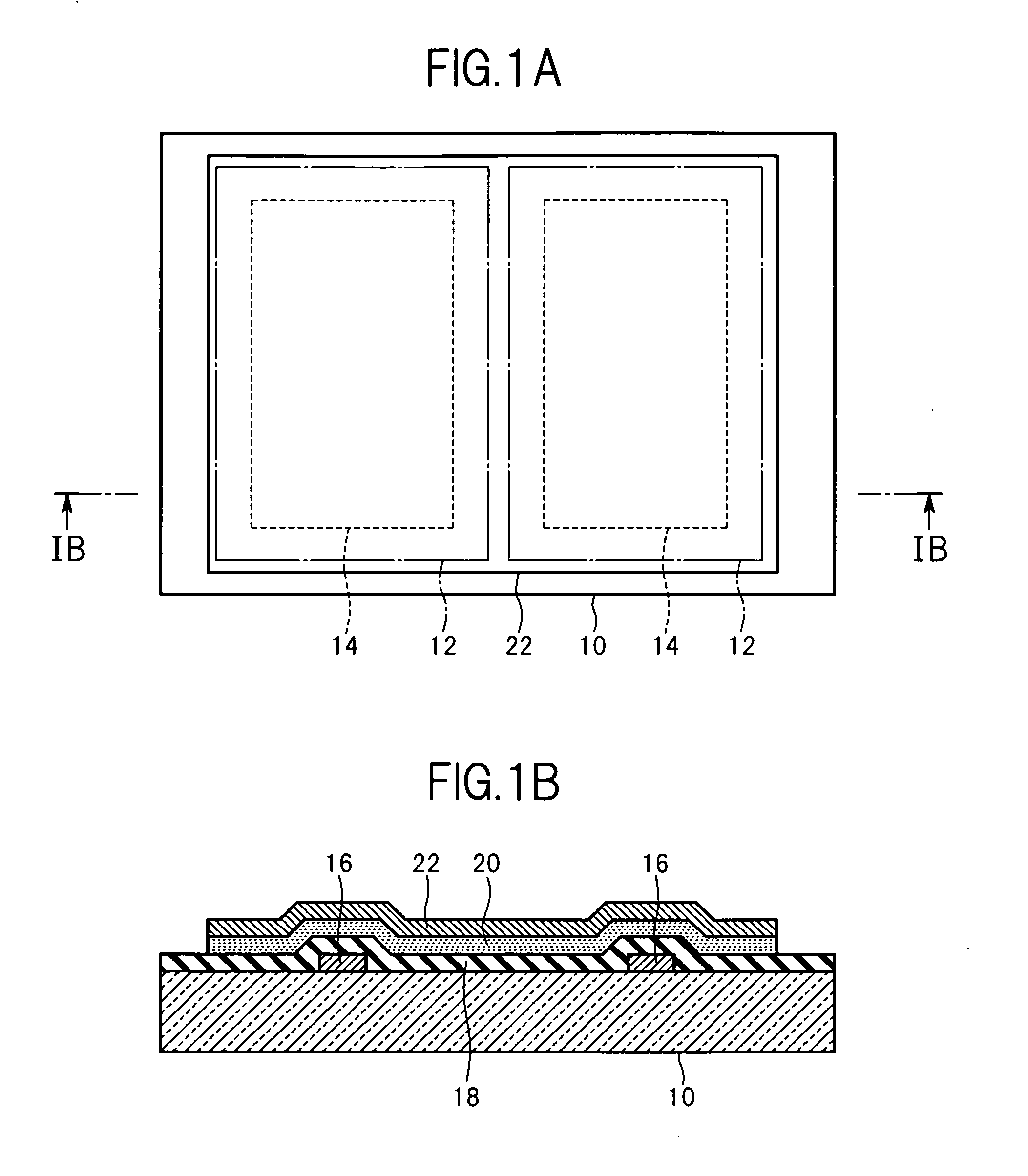
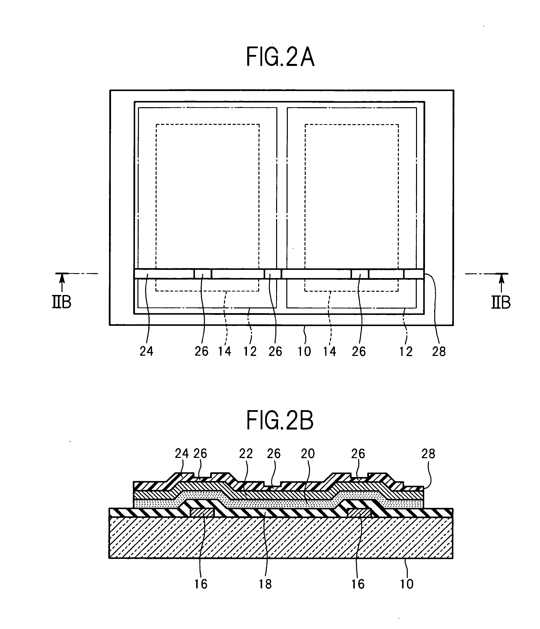
[0070]In this embodiment, as illustrated in FIGS. 1A and 1B, a substrate 10 is prepared. FIG. 1B is a cross-sectional view taken along the line IB-IB of a structure illustrated in FIG. 1A. The substrate 10 is made of glass, for example, and is often required to have optical transparency. The substrate 10 is a mother substrate for manufacturing a plurality of display devices integrally. One substrate 10 has a plurality of product areas 12 (areas corresponding to display device components), and each of the product areas 12 has an effective display area 14 (image display area).

[0071]Taking a liquid crystal display panel as an example of the display device, the substrate 10 is a thin film transistor (TFT) substrate (or array substrate) including thin-film field-effect transistors, pixel electrodes, wirings, and the like. It should be noted that the liq...

second embodiment

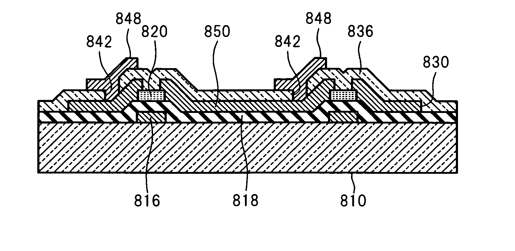
[0093]FIG. 11A to FIG. 13B illustrate a manufacturing method for a display device according to a second embodiment of the present invention. In this embodiment, the same processes as in the first embodiment are performed halfway. Specifically, the processes of the first embodiment described with reference to FIG. 1A to FIG. 6B (up to the process of forming the passivation film 36 over the wiring 30 after the patterning of the wiring 30) are performed. Then, the passivation film 36 is etched before the process of cutting the substrate 10 (see FIGS. 7A and 7B).

[0094]As illustrated in FIGS. 11A and 11B, an etching resist 228 is formed for etching the passivation film 36. FIG. 11B is a cross-sectional view taken along the line XIB-XIB of the structure illustrated in FIG. 11A. The etching resist 228 has first openings 38 and second openings 40, from which the passivation film 36 is exposed. The first openings 38 are formed above the wiring 30 corresponding to portions that need to be ele...

third embodiment

[0099]FIG. 14 to FIG. 24B illustrate a manufacturing method for a display device according to a third embodiment of the present invention. The display device to be manufactured in this embodiment is a liquid crystal display device using two oxide semiconductor layers, such as an in-plane switching (IPS) liquid crystal display device.

[0100]As illustrated in FIG. 14, a first oxide conductive film 552 is formed on a substrate 510. The first oxide conductive film 552 is formed of an oxide semiconductor having conductivity (such as indium tin oxide or indium zinc oxide). The first oxide conductive film 552 is a transparent conductive film. On the first oxide conductive film 552, a first metallic layer 522 is formed.

[0101]FIGS. 15A and 15B are cross-sectional views taken along different lines in the same process. There are similar relationships between FIGS. 16A and 16B, FIGS. 17A and 17B, FIGS. 18A and 18B, FIGS. 21A and 21B, FIGS. 22A and 22B, and FIGS. 23A and 23B, respectively.

[0102]A...


PUM


Abstract

An etching resist including first and second portions, the first portion being thicker than the second portion, is formed on a metallic layer. Through the etching resist, a semiconductor layer and the metallic layer are patterned by etching so as to form a wiring from the metallic layer and leave the semiconductor layer under the wiring. An electrical test is conducted on the wiring. The second portion is removed while the first portion is left unremoved. Selective etching is performed through the first portion so as to leave the semiconductor layer unetched to pattern the wiring to be divided into drain and source electrodes. A substrate is cut. In patterning the wiring, the wiring is etched to be cut at a position closer to a cutting line of the substrate with respect to the drain and source electrodes, while leaving the semiconductor layer unetched.

Description

CROSS-REFERENCE TO RELATED APPLICATION[0001]The present application claims priority from Japanese applications JP 2009-191313 filed on Aug. 20, 2009 and JP 2009-191316 filed on Aug. 20, 2009, the contents of which are hereby incorporated by reference into this application.BACKGROUND OF THE INVENTION[0002]1. Field of the Invention[0003]The present invention relates to a display device and a manufacturing method therefor.[0004]2. Description of the Related Art[0005]It is known to integrally manufacture a plurality of display panels using a mother substrate, and then cut the resultant mother substrate into individual display panels (Japanese Patent Application Laid-open No. Hei 09-138418 and Japanese Patent Application Laid-open No. Hei 10-20288). Taking a liquid crystal display panel as an example, a pair of mother glass substrates are used, in which one mother glass substrate is cut into thin film transistor (TFT) substrates and the other is cut into color filter substrates.[0006]The...

Claims


Application Information

Patent Timeline
Patent Type & Authority Applications(United States)
IPC IPC(8): H01L29/22H01L21/66
CPCH01L22/14H01L29/41733H01L27/1214H01L22/20H01L27/1288
Inventor KAWAMURA, TETSUYASATO, MASASHIWATANABE, YOSHIKIIWATO, HIROAKIHIRATA, MASAFUMI
Owner PANASONIC LIQUID CRYSTAL DISPLAY CO LTD
Why Eureka
Try Eureka