Protective tape separating method and apparatus

a technology of protective tape and separator, applied in the direction of electrical equipment, chemistry apparatus and processes, lamination ancillary operations, etc., can solve the problems of reducing rigidity, reducing rigidity, and affecting the stability of the wafer

Inactive Publication Date: 2011-03-03
NITTO DENKO CORP
View PDF8 Cites 10 Cited by
  • Summary
  • Abstract
  • Description
  • Claims
  • Application Information

AI Technical Summary

Benefits of technology

[0011]The invention discloses a method of separating a protective tape joined to a surface of a substrate. The method includes the steps of reducing an adhesive force of the protective tape joined to the chips into which the substrate having the protective tape joined thereto is diced in a given shape, and separating the protective tape having a reduced adhesive force from the surface of the substrate while suction-holding an entire surface of the substrate.
[0012]With the protective tape separating method of this embodiment, the protective tape is joined to the surface of the substrate from the back grinding process to the process of dicing the substrate into the chips, which results in reinforcement of the substrate. Therefore, damages to the substrate may be suppressed that are likely to occur from the back grinding process to the dicing process.
[0013]Moreover, the protective tape having a reduced adhesive force is separated from the chips. Thus, damages may also be suppressed that are likely to occur upon separation of the protective tape from the thinned substrate of large size. Specifically, the protective tape joined to the chips has a contact area extremely smaller than an area of the protective tape joined to the entire surface of the substrate, which results in a remarkably reduced separation stress on the chips upon separation. Consequently, damages to the chips may be suppressed that occur due to separation stress. The adhesive force in this invention is not limited to that to be reduced, but includes that to be eliminated.
[0015]According to the method of this embodiment, the adhesive force in the adhesion layer of thermal foam is reduced due to heating, and thereafter the protective tape is suction-held by the suction mechanism. Consequently, the protective tape is separated and removed from the chips. Therefore, the protective tape may be removed with high accuracy with no residue of the protective tape on the chips.
[0019]According to the method of this embodiment, the adhesion layer of the protective tape is cured with ultraviolet irradiation, which results in a reduced adhesive force therein.
[0023]According to the configuration of this embodiment, the adhesive force reduction device may reduce the adhesive force in the protective tape on the surface of the chuck table with the chips over the entire surface of the substrate prior to dicing suction-held on the chuck table. Thereafter, the protective tape is separated and removed from the chips.

Problems solved by technology

The above conventional method, however, has the following problem.
The wafer may be damaged under such state.
Moreover, it becomes impossible to reinforce the wafer having reduced rigidity sufficiently only via the dicing tape with respect to the thinned wafer even though the wafer is adhesively held on the dicing tape.
As a result, a new problem arises that the wafer is readily damaged during a step of transporting the mount frame into a dicing process.

Method used


Image

  • Protective tape separating method and apparatus
  • Protective tape separating method and apparatus
  • Protective tape separating method and apparatus

Examples


Embodiment Construction

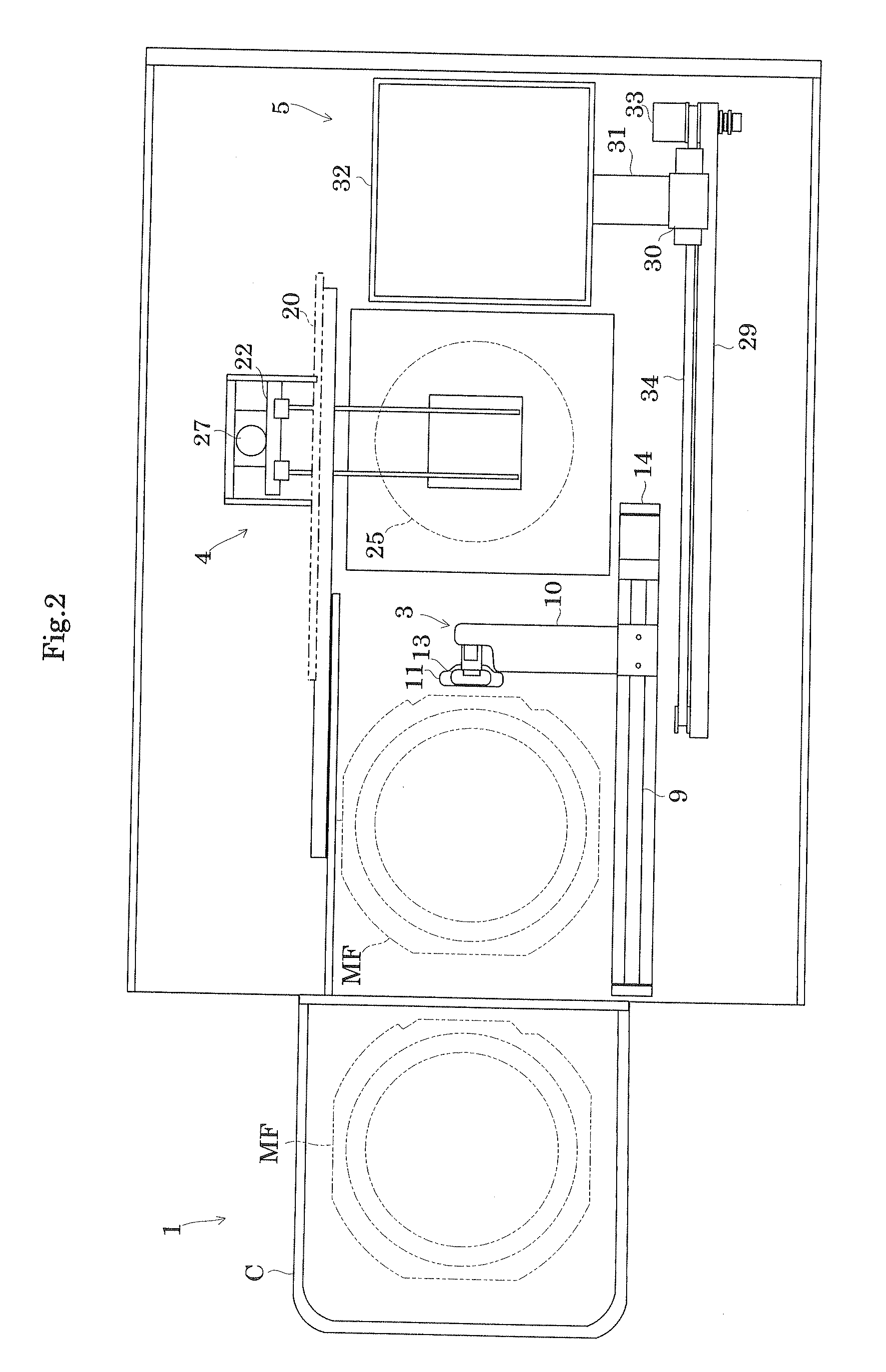
[0045]The invention is described more fully hereinafter with reference to the accompanying drawings, in which embodiments of the invention are shown. This invention may, however, be embodied in many different forms and should not be construed as limited to the embodiments set forth herein. Rather, these embodiments are provided so that this disclosure is thorough, and will fully convey the scope of the invention to those skilled in the art. In the drawings, the size and relative sizes of layers and regions may be exaggerated for clarity. Like reference numerals in the drawings denote like elements.

[0046]One embodiment of this invention will be described hereunder with reference to the drawings.

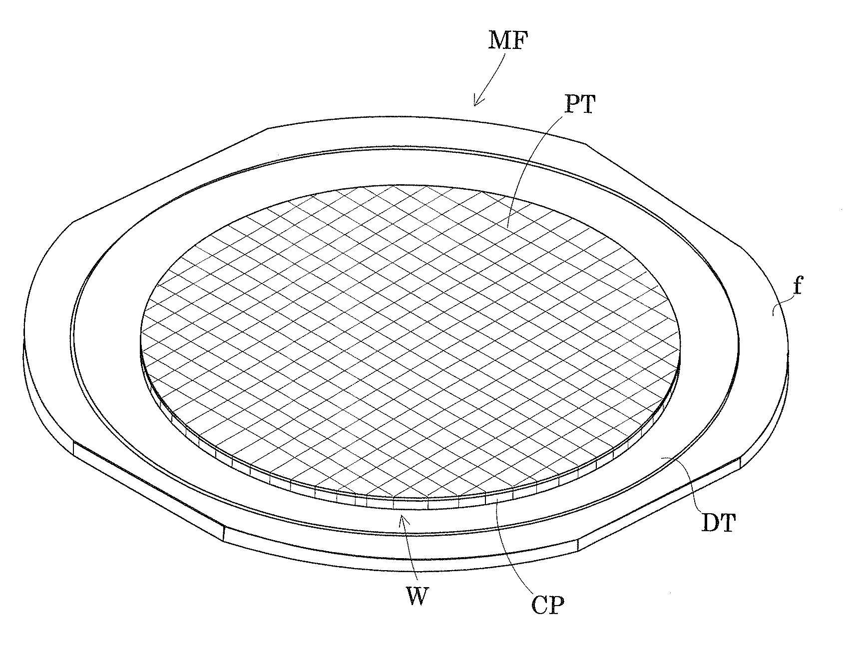
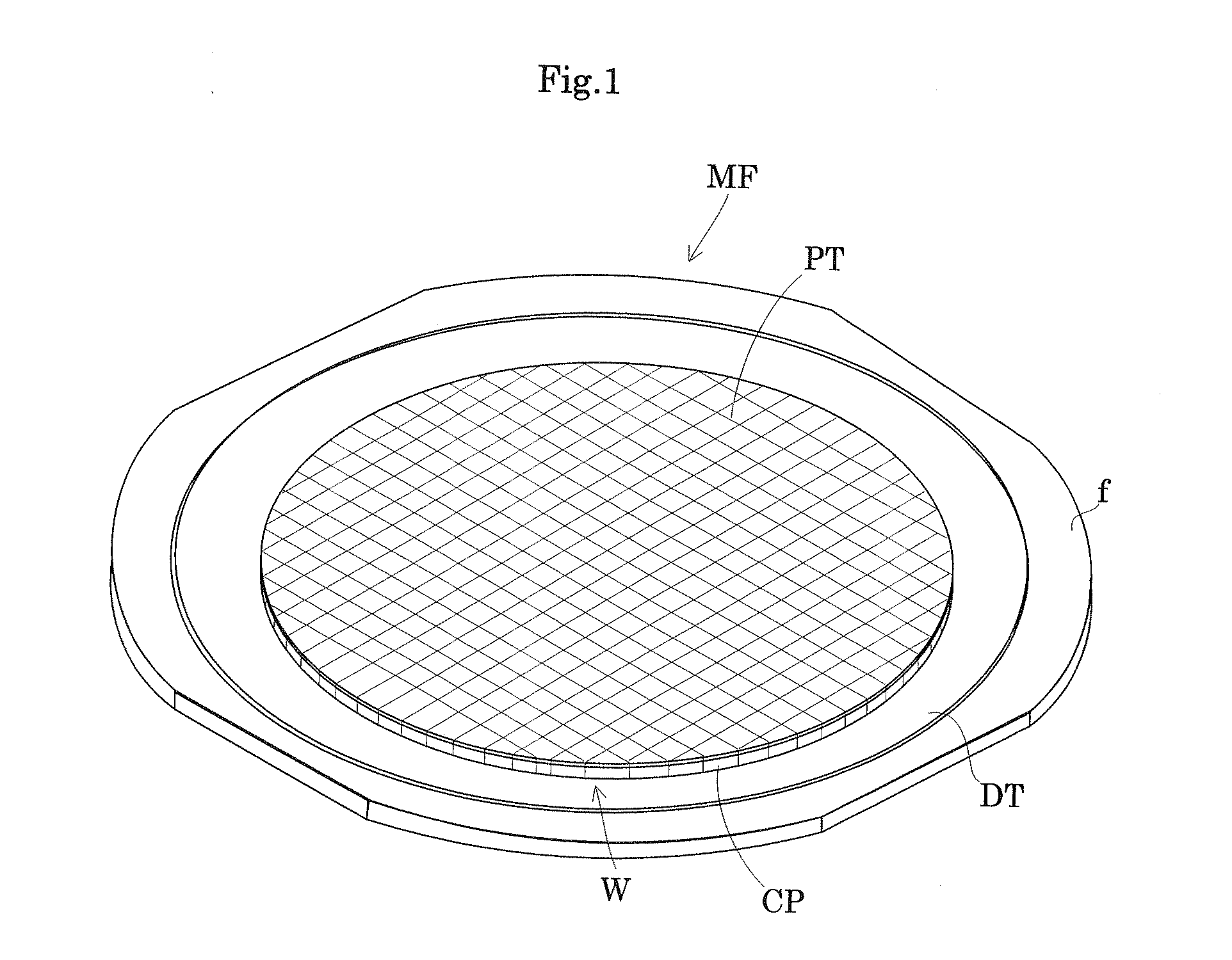
[0047]In this embodiment, a semiconductor wafer is to be described by way of example as a substrate. As shown in FIG. 1, a semiconductor wafer W (hereinafter simply referred to as a “wafer W”) is subject to back grinding and dicing processes with a protective tape PT joined thereto that protec...


PUM

PropertyMeasurementUnit
thicknessaaaaaaaaaa
adhesive forceaaaaaaaaaa
heat shrinkage rateaaaaaaaaaa

Abstract

A chuck table adhesively holds a rear face of a mount frame subject to a dicing process with a protective tape joined thereto, and a suction plate having a heater embedded therein contacts and heats the protective tape. Consequently, an adhesion layer of the protective tape reduces its adhesive force due to foaming and expansion. Thereafter, the suction plate moves upward while keeping its suction force to separate the protective tape from all of chips.

Description

BACKGROUND OF THE INVENTION[0001]1. Field of the Invention[0002]This invention relates to a protective tape separating method and apparatus to separate a protective tape that protects a circuit surface of a substrate such as a semiconductor wafer, a circuit board, and an electron device (for instance, an LED (Light-emitting diode) and a CCD (charge coupled device).) More particularly, this invention is directed to a technique of separating the protective tape from chips produced after dicing of the substrate into a given shape.[0003]2. Description of the Related Art[0004]Typically, numerous components are formed on a surface of a semiconductor wafer (hereinafter simply referred to as a “wafer”), and then grinding is performed to a rear face of the wafer in a back grinding process. Next, the wafer is diced into each component in a dicing process. The wafer tends to be thinned to have a thickness of 100 μm to 50 μm or even less in recent years with a need for a high density package.[0...

Claims


Application Information

Patent Timeline
Patent Type & Authority Applications(United States)
IPC IPC(8): B32B38/10
CPCH01L21/67132Y10T156/1917Y10T156/1153Y10T156/1158Y10T156/1911Y10T156/1147H01L21/6835
Inventor HASE, YUKITOSHIYAMAMOTO, MASAYUKI
Owner NITTO DENKO CORP
Why Eureka
Try Eureka