Power semiconductor device and manufacturing method for the same

a technology of power semiconductor and manufacturing method, which is applied in the direction of semiconductor devices, semiconductor/solid-state device details, electrical equipment, etc., can solve the problems of increasing manufacturing cost or yield, unable to connect an external terminal, and internal components damaged by mold clamping, etc., to achieve the effect of increasing the creeping distance between metal electrode terminals

Active Publication Date: 2011-03-03
MITSUBISHI ELECTRIC CORP
View PDF17 Cites 25 Cited by
  • Summary
  • Abstract
  • Description
  • Claims
  • Application Information

AI Technical Summary

Benefits of technology

[0013]The integral resin sleeve fitted with the electrode terminals protects the electrode terminals from a pressure of the mold in a manufacturing process, whereby it is possible to manufacture a power semiconductor device having a top-exposed electrode structure without strictly controlling dimensions of the internal components and the molds.

Problems solved by technology

However, if a total thickness from the insulating substrate to a tip of the metal electrode terminal is larger than a length of an inside of a cavity in a longitudinal direction, unfortunately, internal components are damaged by mold clamping.
As a result, the metal electrode terminal is not exposed to the outside of the molding resin after injection of the molding resin, which makes it unable to connect an external terminal.
In order to avoid such problems, it is required to strictly control accuracy of dimension of internal components such as an insulating substrate, a power semiconductor, a metal electrode terminal, solder, and a mold, which causes an increase in manufacturing cost or a decrease in yield.
Nevertheless, creeping discharge occurs if a creeping distance between the metal electrode terminals is excessively small, and hence the creeping distance imposes a limitation on further miniaturization.

Method used


Image

  • Power semiconductor device and manufacturing method for the same
  • Power semiconductor device and manufacturing method for the same
  • Power semiconductor device and manufacturing method for the same

Examples


first preferred embodiment

[0039](Configuration)

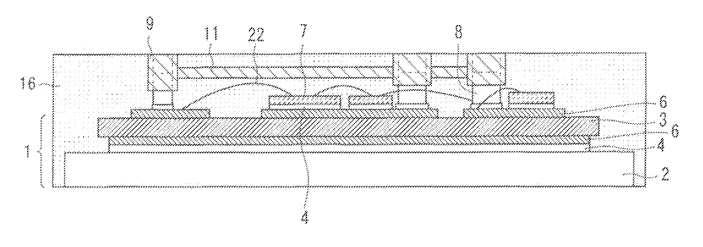
[0040]FIG. 1 shows an example of a sectional view of a power semiconductor device according to a first preferred embodiment. The power semiconductor device according to the first preferred embodiment includes an insulating substrate 1 on which a circuit pattern 6 is formed, a power semiconductor 7 and metal socket electrode terminals 8 which are formed on the circuit pattern 6 of the insulating substrate 1, and an integral resin sleeve 10 fitted with the metal socket electrode terminals 8.

[0041]The insulating substrate 1 is composed of a base plate 2 and a ceramic substrate 3 formed through solder 4 on the base plate 2. The base plate 2 functions as a heat spreader for promoting heat dissipation of the power semiconductor 7 or the like, and a back surface thereof is exposed from a molding resin 16. For example, aluminum (Al), copper (Cu), aluminum silicon carbide (AlSiC), copper-molybdenum (Cu—Mo) or the like is used as a material therefor.

[0042]That is, the ins...

second preferred embodiment

[0100](Configuration)

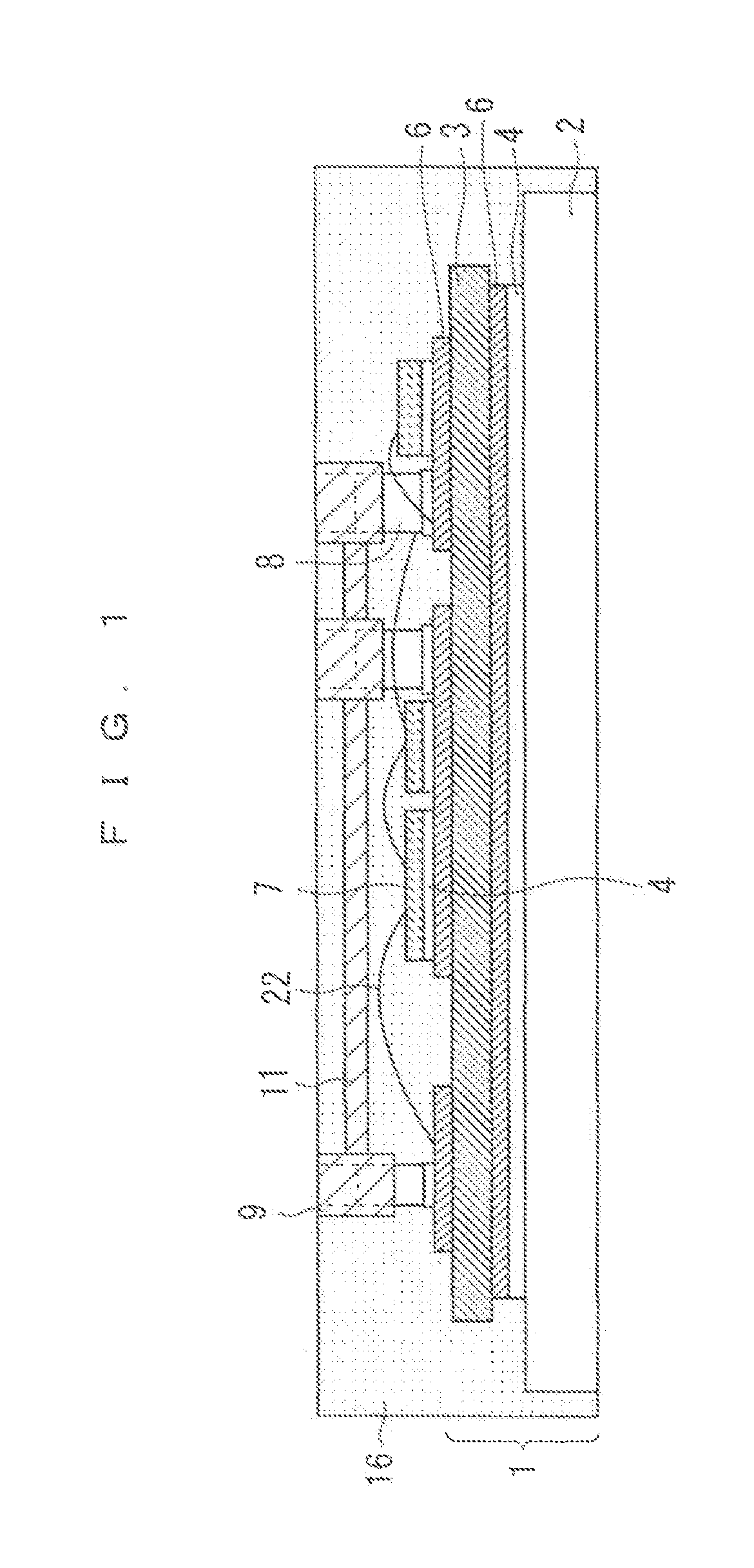
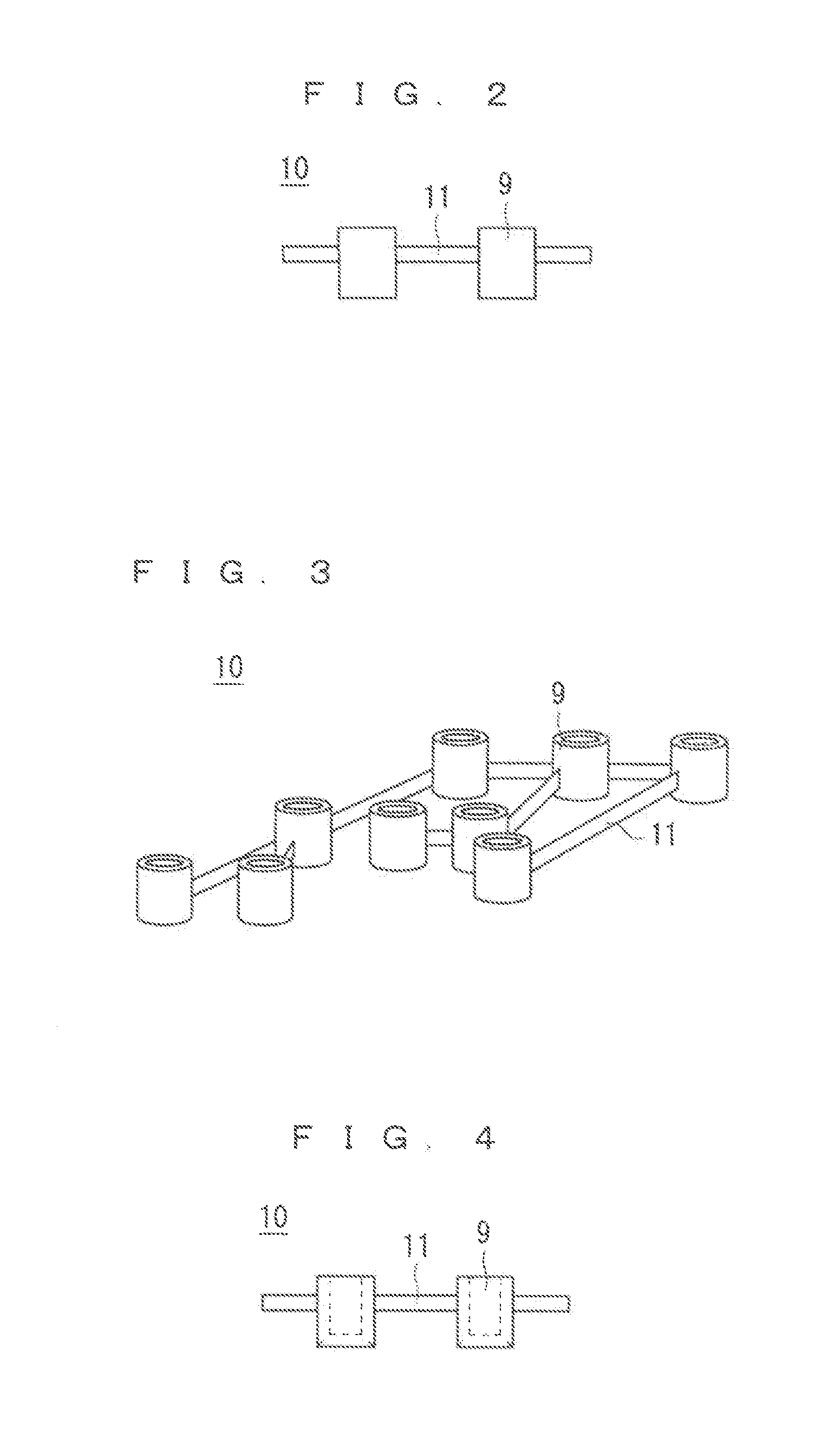
[0101]FIG. 10 is a sectional view showing a configuration of a power semiconductor device according to a second preferred embodiment. The components similar to those of the first preferred embodiment, which are shown in FIG. 1, are denoted by the same reference numerals. The power semiconductor device according to the second preferred embodiment is different from the power semiconductor device according to the first preferred embodiment in the structure of the integral resin sleeve 10. While the rod-like runner part 11 couples the sleeve parts 9 in the first preferred embodiment, in the second preferred embodiment, a plurality of sleeve parts 9 are formed on a resin flat plate 12 to form the integrate resin sleeve 10, as shown in FIG. 11. The configuration other than this is similar to that of the first preferred embodiment.

[0102]That is, the integral resin sleeve 10 has the structure in which a plurality of sleeve parts 9 are formed on the resin flat plate 12. ...

third preferred embodiment

[0126](Configuration)

[0127]FIG. 22 is a sectional view showing a configuration of a power semiconductor device according to a third preferred embodiment. The components similar to those of the first preferred embodiment shown in FIG. 1 are denoted by the same reference numerals. In the power semiconductor device according to the third preferred embodiment, an insulating heat-conductive sheet 5 is used in place of the ceramic substrate 3 used in the power semiconductor device according to the first preferred embodiment. The base plate 2 and the circuit pattern 6 are integrated through the insulating heat-conductive sheet 5. The configuration other than this is similar to that of the first preferred embodiment, and therefore its description is omitted.

[0128](Effect)

[0129]In the power semiconductor device according to the third preferred embodiment, the insulating substrate 1 is composed of the base plate 2 and the insulating heat-conductive sheet 5 on which the circuit pattern 6 is fo...


PUM


Abstract

Provided is a power semiconductor device including: an insulating substrate; a circuit pattern formed on an upper surface of the insulating substrate; a power semiconductor formed on the circuit pattern; a plurality of metal socket electrode terminals formed perpendicularly to the circuit pattern or the power semiconductor so as to be in conduction with external terminals; an integral resin sleeve in which a plurality of sleeve parts are integrated, the plurality of sleeve parts being fitted with the plurality of metal socket electrode terminals from above the plurality of metal socket electrode terminals and having openings at both ends thereof; and a molding resin covering the insulating substrate, the circuit pattern, the power semiconductor, the electrode terminals, and the integral resin sleeve.

Description

BACKGROUND OF THE INVENTION[0001]1. Field of the Invention[0002]The present invention relates to a transfer-molding type power semiconductor device and a manufacturing method for the same, and more particularly, to a power semiconductor device in which metal socket electrode terminals for top-exposed electrodes are arranged perpendicularly to an insulating substrate and a manufacturing method for the same.[0003]2. Description of the Background Art[0004]In many cases, typical semiconductor packages are formed by resin sealing including transfer-molding in terms of manufacturing cost, productivity or the like. In the transfer molding, a resin composition (molding resin) is melted by high-frequency heating as required, and then is filled into a hollow (cavity) inside a metal mold kept at high temperature. The metal mold is typically composed of an upper mold and a lower mold combined therewith, and the cavity is defined by inner walls of the upper and lower molds. A plunger is used for...

Claims


Application Information

Patent Timeline
Patent Type & Authority Applications(United States)
IPC IPC(8): H01L23/28H01L21/50
CPCH01L21/565H01L2224/49H01L24/28H01L24/29H01L24/45H01L24/48H01L24/49H01L25/072H01L2224/32225H01L2224/45124H01L2224/48091H01L2224/48137H01L2224/48227H01L2224/48237H01L2224/73265H01L2224/92247H01L2924/01014H01L2924/014H01L2924/10272H01L2924/13055H01L2924/13091H01L23/3121H01L2924/01079H01L2924/01068H01L2924/01013H01L2924/1305H01L2924/00014H01L2924/00H01L2924/00012H01L24/73H01L2924/181
Inventor OKA, SEIJIYAMAGUCHI, YOSHIHIRO
Owner MITSUBISHI ELECTRIC CORP
Why Eureka
Try Eureka