
Liquid crystal display device

a liquid crystal display and display device technology, applied in the direction of instruments, transportation and packaging, chemistry apparatus and processes, etc., can solve problems such as image sticking, and achieve the effect of high transmittan

Active Publication Date: 2011-03-03
PANASONIC LIQUID CRYSTAL DISPLAY CO LTD +1
View PDF7 Cites 43 Cited by
  • Summary
  • Abstract
  • Description
  • Claims
  • Application Information

AI Technical Summary

Benefits of technology

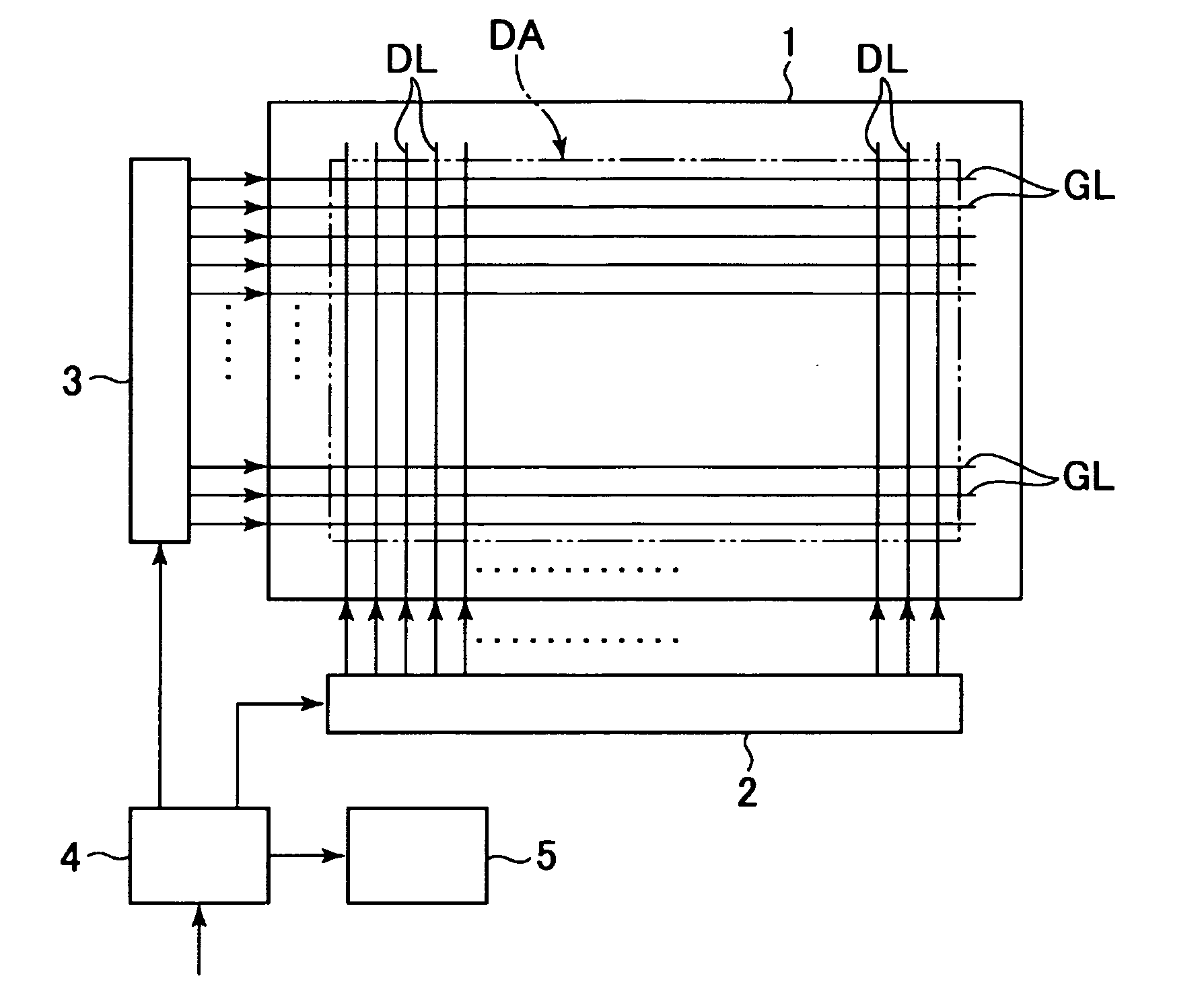
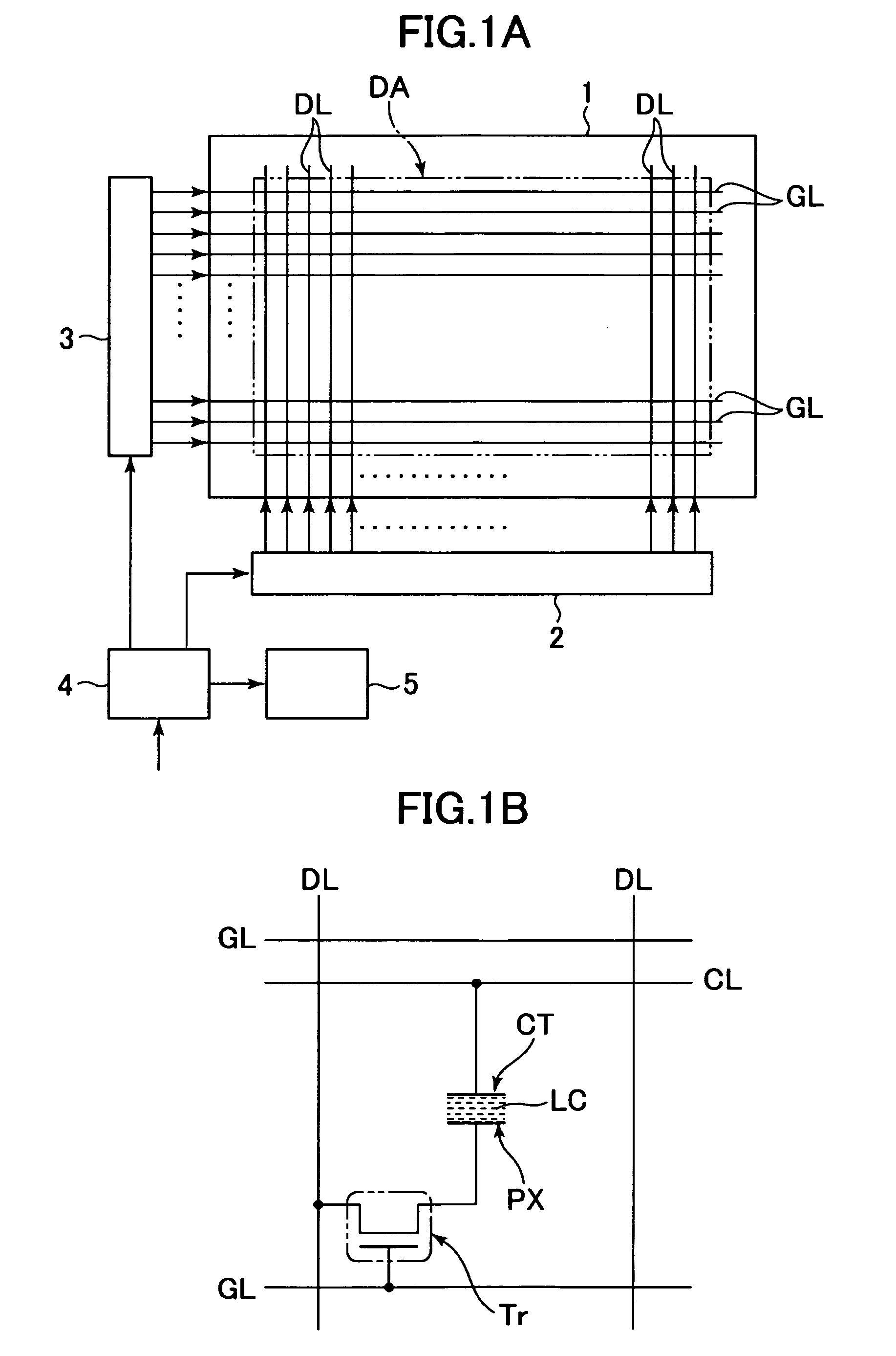
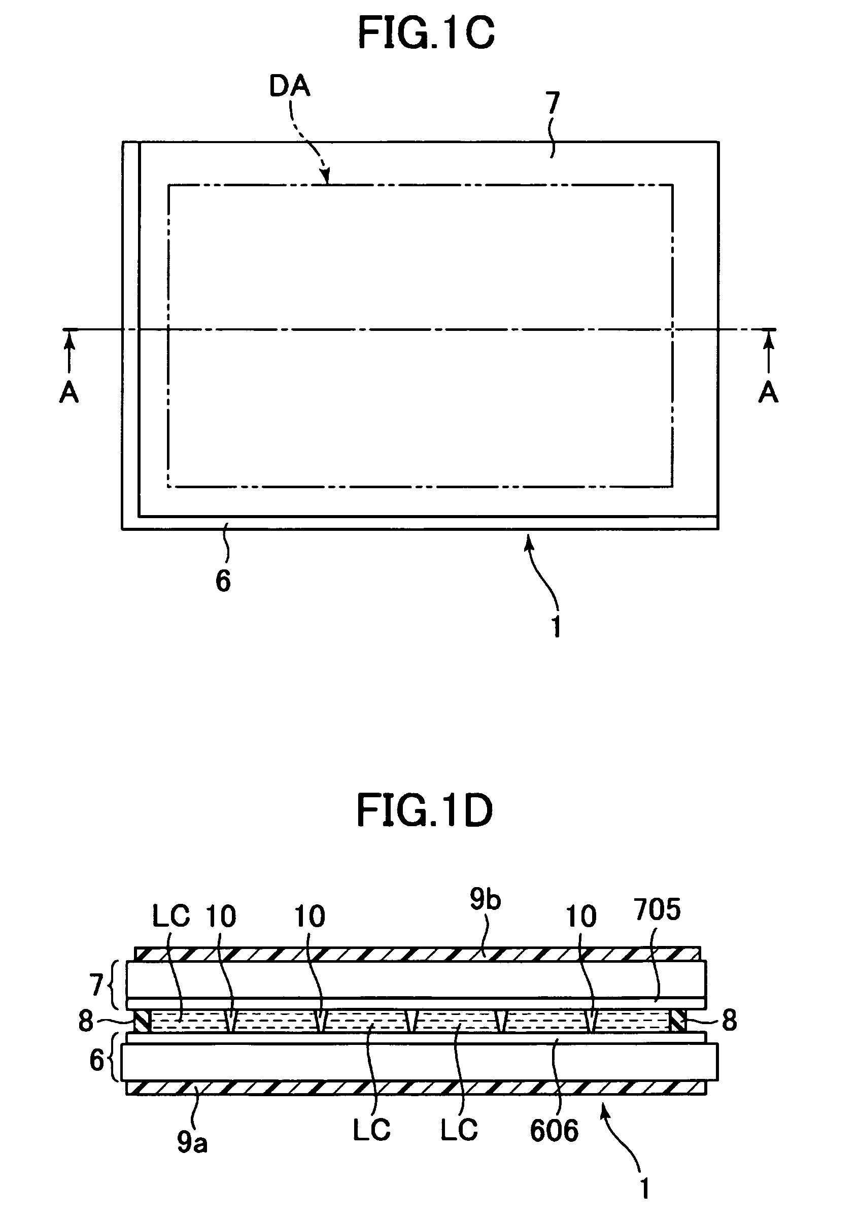
[0024]According to the present invention, there may be provided a liquid crystal display device of high transmittance in which image sticking of displayed images is inhibited.

Problems solved by technology

In liquid crystal display devices, image sticking may happen when, for example, the same image is kept displayed for a long time, and the image faintly remains on the screen after the screen switches to the next image.

Method used


Image

  • Liquid crystal display device
  • Liquid crystal display device
  • Liquid crystal display device

Examples


example 1

[0067]FIGS. 2A to 2F are schematic diagrams illustrating the schematic structure of an in-plane switching (IPS) liquid crystal panel according to Example 1 of the present invention. FIG. 2A is a schematic plan view illustrating the planar structure of a single pixel of an active matrix substrate (first substrate) 6 in the liquid crystal panel of Example 1. FIG. 2B is a schematic plan view illustrating the planar structure of the pixel in which a counter substrate (second substrate) is laid on top of an area illustrated in FIG. 2A. FIG. 2C is a schematic sectional view illustrating a sectional structure cut along the lines B-B of FIGS. 2A and 2B. FIG. 2D is a schematic sectional view illustrating an example of a sectional structure cut along the lines C-C of FIGS. 2A and 2B. FIG. 2E is a schematic sectional view illustrating a sectional structure cut along the lines D-D of FIGS. 2A and 2B. FIG. 2F is a schematic sectional view illustrating a sectional structure cut along the lines E-...

example 2

[0103]FIGS. 3A to 3C are schematic diagrams illustrating an example of the schematic structure of an FFS liquid crystal panel according to Example 2 of the present invention.

[0104]FIG. 3A is a schematic plan view illustrating the planar structure of a single pixel of an active matrix substrate (first substrate) in the liquid crystal panel of Example 2. FIG. 3B is a schematic sectional view illustrating a sectional structure cut along the line F-F of FIG. 3A. FIG. 3C is a schematic sectional view illustrating a sectional structure cut along the line G-G of FIG. 3A. FIGS. 3B and 3C also illustrate the sectional structure of the liquid crystal layer LC (liquid crystal material) and the second substrate 7 which are located above the first substrate 6.

[0105]Example 2 takes a lateral field driving liquid crystal panel as an example of the liquid crystal panel 1 according to the present invention. In the liquid crystal panel 1 of Example 2, a single pixel and its surroundings are structure...

example 3

[0127]FIG. 4 is a schematic sectional view illustrating the sectional structure of a main part of a VA liquid crystal panel according to Example 3 of the present invention.

[0128]Example 3 takes a vertical field driving liquid crystal panel as an example of the liquid crystal panel 1 to which the present invention is applied. The vertical field driving liquid crystal panel 1 is structured, for example, as illustrated in FIG. 4, where the pixel electrode PX is formed on the first substrate 6 and the common electrode CT is formed on the second substrate 7.

[0129]In the case where the liquid crystal panel 1 employs VA, which is one of the vertical field driving methods, the pixel electrode PX and the common electrode CT are formed from a transparent conductor such as ITO into a simple flat shape. The liquid crystal molecules 11 in this case are aligned vertically with respect to the surfaces of the glass substrates 601 and 701 by the first alignment film 606 and the second alignment film...


PUM

PropertyMeasurementUnit
volume resistivityaaaaaaaaaa
thicknessaaaaaaaaaa

Abstract

Provided is a liquid crystal display device includes: a first substrate (6); a second substrate (7); a liquid crystal layer (LC); a first alignment film (606) placed on the first substrate; a second alignment film (705) placed on the second substrate; and at least one of: a transparent layer (610) contacting the first alignment film on the other side of the liquid crystal layer and being lower in volume resistivity than the first alignment film; and a transparent layer (710) contacting the second alignment film on the other side of the liquid crystal layer and being lower in volume resistivity than the second alignment film, wherein the transparent layer contains polysiloxane expressed by Chemical Formula 1:where R1 and R2 each represent an alkyl group or alkoxy group having 1 to 3 carbon atoms, or a hydroxyl group, and at least 30% of hydroxyl groups are contained.

Description

CROSS-REFERENCE TO RELATED APPLICATION[0001]The present application claims priority from Japanese application JP2009-200758 filed on Aug. 31, 2009, the content of which is hereby incorporated by reference into this application.BACKGROUND OF THE INVENTION[0002]1. Field of the Invention[0003]The present invention relates to a liquid crystal display device that includes an alignment film for aligning liquid crystal molecules in a liquid crystal layer which is sandwiched between two substrates.[0004]2. Description of the Related Art[0005]Liquid crystal display devices are being applied to increasingly wide range of uses because of their features such as high display quality, thinness, light weight, and low power consumption. The various uses of liquid crystal display devices include monitors for portable devices, e.g., cell phone monitors and digital still camera monitors, monitors for desktop personal computers, monitors for printing and designing, monitors for medical practice, and li...

Claims


Application Information

Patent Timeline
Patent Type & Authority Applications(United States)
IPC IPC(8): G02F1/1337
CPCG02F1/134363G02F2001/134372G02F1/133345G02F1/133711G02F1/133723G02F1/133788Y10T428/1005G02F2001/133796G02F2001/134381G02F2202/022G02F2202/16Y10T428/10Y10T428/1036G02F2001/133397C09K2323/03C09K2323/02C09K2323/00G02F1/133397G02F1/133796G02F1/134372G02F1/134381
Inventor MATSUMORI, MASAKITOMIOKA, YASUSHI
Owner PANASONIC LIQUID CRYSTAL DISPLAY CO LTD
Learn More