Latency counter, semiconductor memory device including the same, and data processing system

a technology of latency counter and semiconductor memory device, applied in the field of latency counter, to achieve the effect of reducing circuit scale and power consumption

Active Publication Date: 2011-03-10
LONGITUDE LICENSING LTD
View PDF8 Cites 2 Cited by
  • Summary
  • Abstract
  • Description
  • Claims
  • Application Information

AI Technical Summary

Benefits of technology

[0009]According to the present invention, a command latched in a point-shift FIFO circuit is reset in response to a count value that is different from the count value corresponding to the counter circuit. Consequently, there is no need to provide a circuit or the like in each of the latch circuits for generating a one-shot pulse for resetting the latch circuit. As a result, the circuit scale and power consumption can be reduced.

Problems solved by technology

However, even in the synchronous DRAM, operations performed by the DRAM core are only analog, and therefore it becomes necessary to amplify a very weak electric charge by performing a sense operation.

Method used


Image

  • Latency counter, semiconductor memory device including the same, and data processing system
  • Latency counter, semiconductor memory device including the same, and data processing system
  • Latency counter, semiconductor memory device including the same, and data processing system

Examples


Embodiment Construction

[0024]Preferred embodiments of the present invention will be explained below in detail with reference to the accompanying drawings.

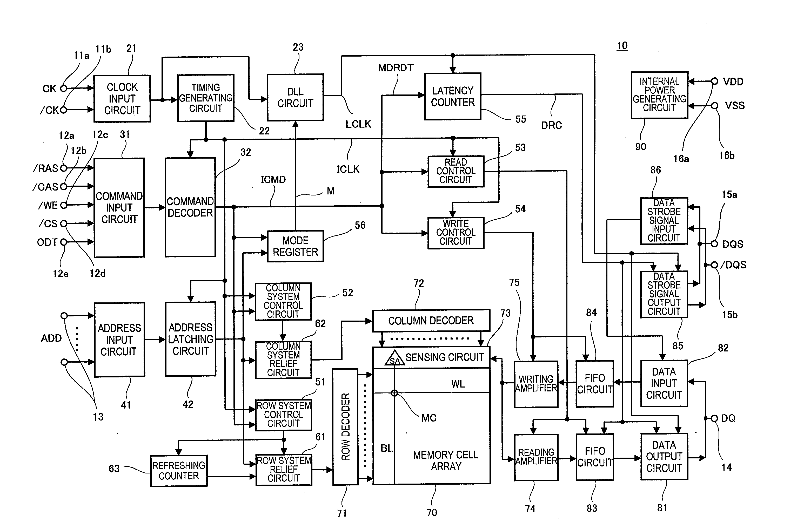
[0025]FIG. 1 is a block diagram showing whole constitution of a semiconductor memory device 10 according to an embodiment of the present invention.

[0026]The semiconductor memory device 10 according to the present embodiment is a synchronous DRAM. The semiconductor memory device 10 includes, as external terminals, clock terminals 11a and 11b, command terminals 12a to 12e, address terminals 13, a data input and output terminal 14, data strobe terminals 15a and 15b, and power terminals 16a and 16b.

[0027]The clock terminals 11a and 11b are terminals to which clock signals CK and / CK are supplied, respectively. These clock signals CK and / CK are then supplied to a clock input circuit 21. In this specification, a signal with a “ / (slash)” at the beginning of the signal name means that the signal is an inverse signal or a low-active signal of a corresponding si...


PUM


Abstract

A latency counter includes an input selecting circuit that selects one of a plurality of signal paths and supplies an internal command to the selected signal path, a shift circuit that switches a correspondence relation between the signal paths and a latch circuit, and an output selecting circuit that causes the internal command taken in the latch circuit to be output. The input selection circuit includes a timing control circuit allocated to each of the signal paths. The timing control circuit includes an SR latch circuit that is set by the internal command and is reset in response to deactivation of a corresponding count value. Therefore, it becomes possible to suppress shortening of an active period of the internal command that is output from the input selecting circuit.

Description

BACKGROUND OF THE INVENTION[0001]1. Field of the Invention The present invention relates to a latency counter, and more particularly relates to a latency counter that counts a latency of an internal command within a synchronous memory. The present invention also relates to a semiconductor memory device including the latency counter, and a data processing system including the semiconductor memory device.[0002]2. Description of Related Art[0003]A synchronous memory represented by a synchronous DRAM (Dynamic Random Access Memory) is widely used for a main memory of a personal computer or the like. Because the synchronous memory can input and output data in synchronization with a clock signal supplied from a controller, a data transfer rate can be increased by using a faster clock.[0004]However, even in the synchronous DRAM, operations performed by the DRAM core are only analog, and therefore it becomes necessary to amplify a very weak electric charge by performing a sense operation. Du...

Claims


Application Information

Patent Timeline
Patent Type & Authority Applications(United States)
IPC IPC(8): G11C8/18G11C8/04
CPCG11C11/4076G11C2207/2272G11C11/4094
Inventor FUJISAWA, HIROKI
Owner LONGITUDE LICENSING LTD
Why Eureka
Try Eureka