Wobble signal processing apparatus

a signal processing and wobble technology, applied in the field of signal processing system, can solve the problems of easy affecting of analog processing of conventional wobble signal processing apparatus, and deterioration of filter characteristics, so as to improve signal processing quality and reduce circuit scale and power consumption

Inactive Publication Date: 2008-02-05
PANASONIC CORP
View PDF11 Cites 5 Cited by
  • Summary
  • Abstract
  • Description
  • Claims
  • Application Information

AI Technical Summary

Benefits of technology

[0004]Accordingly, an object of the present invention is to provide a wobble signal processing apparatus that can reduce the circuit scale and the power consumption, and improve the quality of signal processing.

Problems solved by technology

However, the analog processing of the conventional wobble signal processing apparatus is easily affected by processing variations in the semiconductor processing and, for example, the resistance or capacitance value may deviate from a set value by several to a dozen or more percent.
In addition, deviation of a supply voltage value in the power supply unit may cause a fatal problem in the analog system that requires a fine set value.
For example, when a filter parameter such as the cutoff frequency of a BPF (Band pass filter) or LPF (Low pass filter) deviates, the filter characteristics are deteriorated.
When the power supply value of an analog unit cannot obtain a set value with stability, the supply voltage characteristics vary, and then the filter characteristics are deteriorated.
Further, as the delay amount varies in the analog system, a circuit for phase compensation is required, thereby adversely increasing the circuit scale and the power consumption.

Method used


Image

  • Wobble signal processing apparatus
  • Wobble signal processing apparatus
  • Wobble signal processing apparatus

Examples


first embodiment

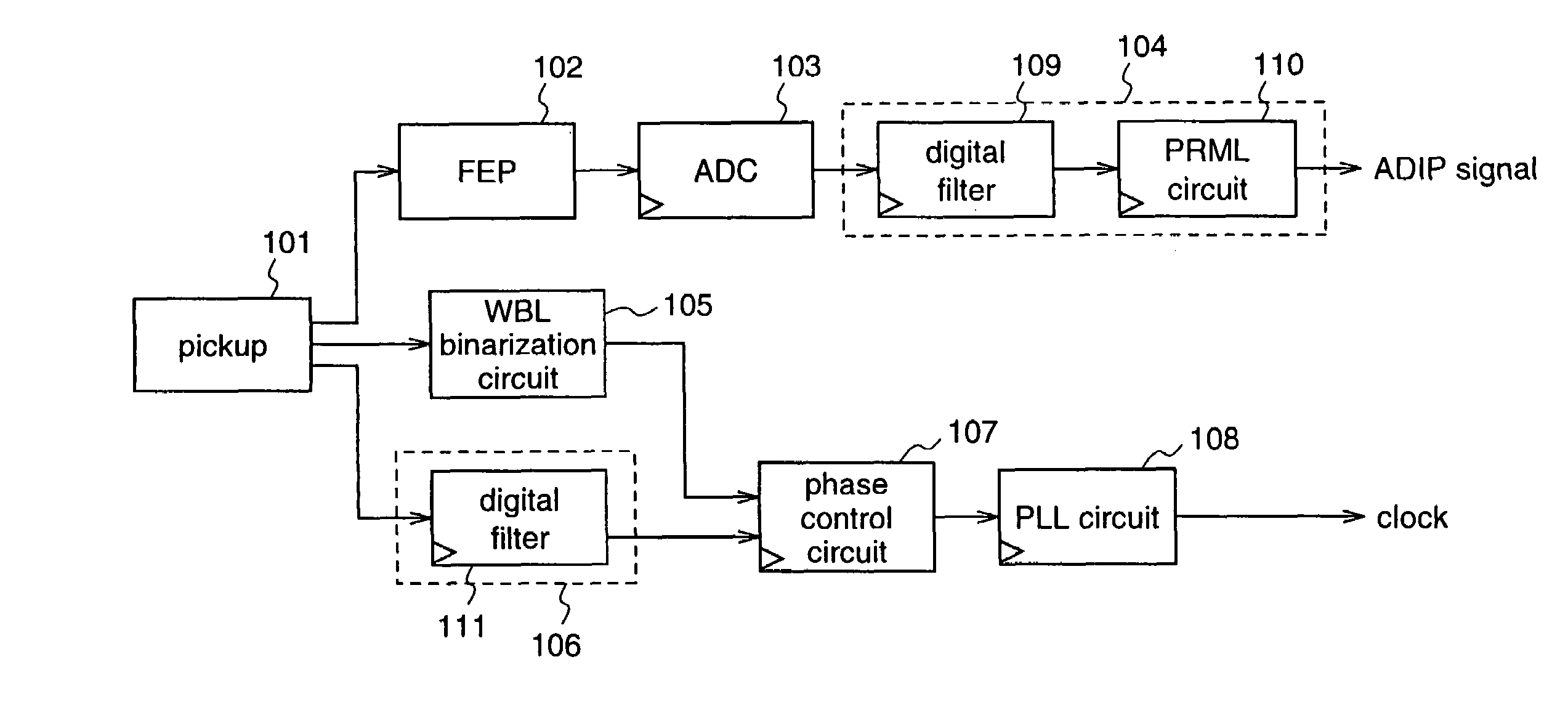
[0037]A wobble signal processing apparatus according to a first embodiment of the present invention will now be described.

[0038]FIG. 1 is a block diagram illustrating a construction of the wobble signal processing apparatus according to the first embodiment. In FIG. 1, the wobble signal processing apparatus according to the first embodiment is constituted by a pickup 101, a FEP (Front End Processor) 102, an ADC (Analog-to-Digital Converter) 103, an address detection circuit 104, a WBL binarization circuit 105, a waveform shaping circuit 106, a phase control circuit 107, and a PLL (Phase Locked Loop) circuit 108.

[0039]The pickup 101 outputs a wobble signal (hereinafter, referred to as a WBL signal) read from a recording medium to the FEP 102, outputs a wobble binary signal (hereinafter, referred to as a WBL binary signal) to the WBL binarization circuit 105, and outputs a RF signal to the waveform shaping circuit 106, respectively. The pickup 101 may include an aperture ratio decisio...

second embodiment

[0088]A wobble signal processing apparatus according to a second embodiment of the present invention will now be described.

[0089]FIG. 8 is a block diagram illustrating a construction of the wobble signal processing apparatus according to the second embodiment. In FIG. 8, the wobble signal processing apparatus according to the second embodiment comprises a pickup 101, a PEP 102, an ADC 103, an address detection circuit 201, a WBL binarization circuit 105, a waveform shaping circuit 106, a phase control circuit 107, and a PLL circuit 108.

[0090]The wobble signal processing apparatus of the second embodiment is different from the above-mentioned wobble signal processing apparatus of the first embodiment in the construction of the address detection circuit 201, and the same components as those in the wobble signal processing apparatus of the first embodiment are denoted by the same reference numerals.

[0091]The address detection circuit 201 comprises a digital filter 109, a phase control ...

third embodiment

[0107]A wobble signal processing apparatus according to a third embodiment of the present invention will now be described.

[0108]FIG. 10 is a block diagram illustrating a construction of a wobble signal processing apparatus according to the third embodiment of the present invention. In FIG. 10, the wobble signal processing apparatus comprises a pickup 101, a FEP 102, an ADC 103, an address detection circuit 301, a WBL binarization circuit 105, a waveform shaping circuit 106, a phase control circuit 107, and a PLL circuit 108.

[0109]The wobble signal processing apparatus according to the third embodiment is different from the wobble signal processing apparatus of the first embodiment in the construction of the address detection circuit 301, and the same components as those in the wobble signal processing apparatus of the first embodiment are denoted by the same reference numerals.

[0110]The address detection circuit 301 is constituted by a digital filter 109 and a DSV (Digital Sum Value...


PUM

PropertyMeasurementUnit
phaseaaaaaaaaaa
distanceaaaaaaaaaa
thresholdaaaaaaaaaa

Abstract

The present invention is made to improve the conventional analog processing that is easily affected by variations in semiconductor processing. This invention provides a wobble signal processing apparatus that can reduce the circuit scale and the power consumption as well as improve the quality of signal processing. The wobble signal processing apparatus of the present invention digitally processes a part that has conventionally been processed by an analog system, and a PRML circuit is further provided to implement error detection, whereby the circuit scale and the power consumption is reduced. This improves the detection of a signal that is inputted to the wobble signal processing apparatus.

Description

FIELD OF THE INVENTION[0001]The present invention relates to a signal processing system in the technology of digital signal processing for optical discs (recording media).BACKGROUND OF THE INVENTION[0002]In conventional wobble signal processing apparatus, means for processing signals by an analog system are utilized (see, for example, Japanese Examined Patent Publication No. Hei.6-19898). As methods for phase-modulating wobbles on tracks by these conventional wobble signal processing apparatus, methods such as BPSK, DPSK, and QPSK have been proposed.[0003]However, the analog processing of the conventional wobble signal processing apparatus is easily affected by processing variations in the semiconductor processing and, for example, the resistance or capacitance value may deviate from a set value by several to a dozen or more percent. In addition, deviation of a supply voltage value in the power supply unit may cause a fatal problem in the analog system that requires a fine set value...

Claims


Application Information

Patent Timeline
Patent Type & Authority Patents(United States)
IPC IPC(8): G11B7/00G11B7/005G11B7/007G11B20/14G11B20/10H03M7/14
CPCG11B7/0053
Inventor MOURI, HIROKIOKAMOTO, KOUJIOGURA, YOUICHI
Owner PANASONIC CORP
Why Eureka
Try Eureka