
Single-Chip Flash Device with Boot Code Transfer Capability

a single-chip, flash device technology, applied in the direction of memory address/allocation/relocation, program control, instruments, etc., can solve the problems of flash card manufacturer significant inventory problems, code may have to be updated, and the boot code and/or control code can have bugs

Inactive Publication Date: 2011-03-17
SUPER TALENT TECH CORP
View PDF4 Cites 100 Cited by
  • Summary
  • Abstract
  • Description
  • Claims
  • Application Information

AI Technical Summary

Problems solved by technology

A problem with conventional flash memory systems is that the boot code and / or the control code can have bugs, which may not be discovered until the flash memory system is already in the field.
Also, the boot code and / or the control code may have to be updated due to bugs or due to improvements to the codes.
A problem with this solution is that it can cause significant inventory issues for a flash card manufacturer.
This can be an on-going problem if subsequent updates are required.

Method used


Image

  • Single-Chip Flash Device with Boot Code Transfer Capability
  • Single-Chip Flash Device with Boot Code Transfer Capability
  • Single-Chip Flash Device with Boot Code Transfer Capability

Examples


Embodiment Construction

The present invention relates to an improvement in flash memory systems. The following description is presented to enable one of ordinary skill in the art to make and use the invention as provided in the context of a particular application and its requirements. Various modifications to the preferred embodiment will be apparent to those with skill in the art, and the general principles defined herein may be applied to other embodiments. Therefore, the present invention is not intended to be limited to the particular embodiments shown and described, but is to be accorded the widest scope consistent with the principles and novel features herein disclosed.

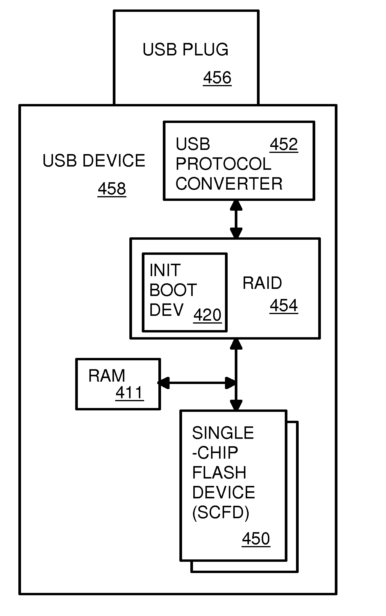
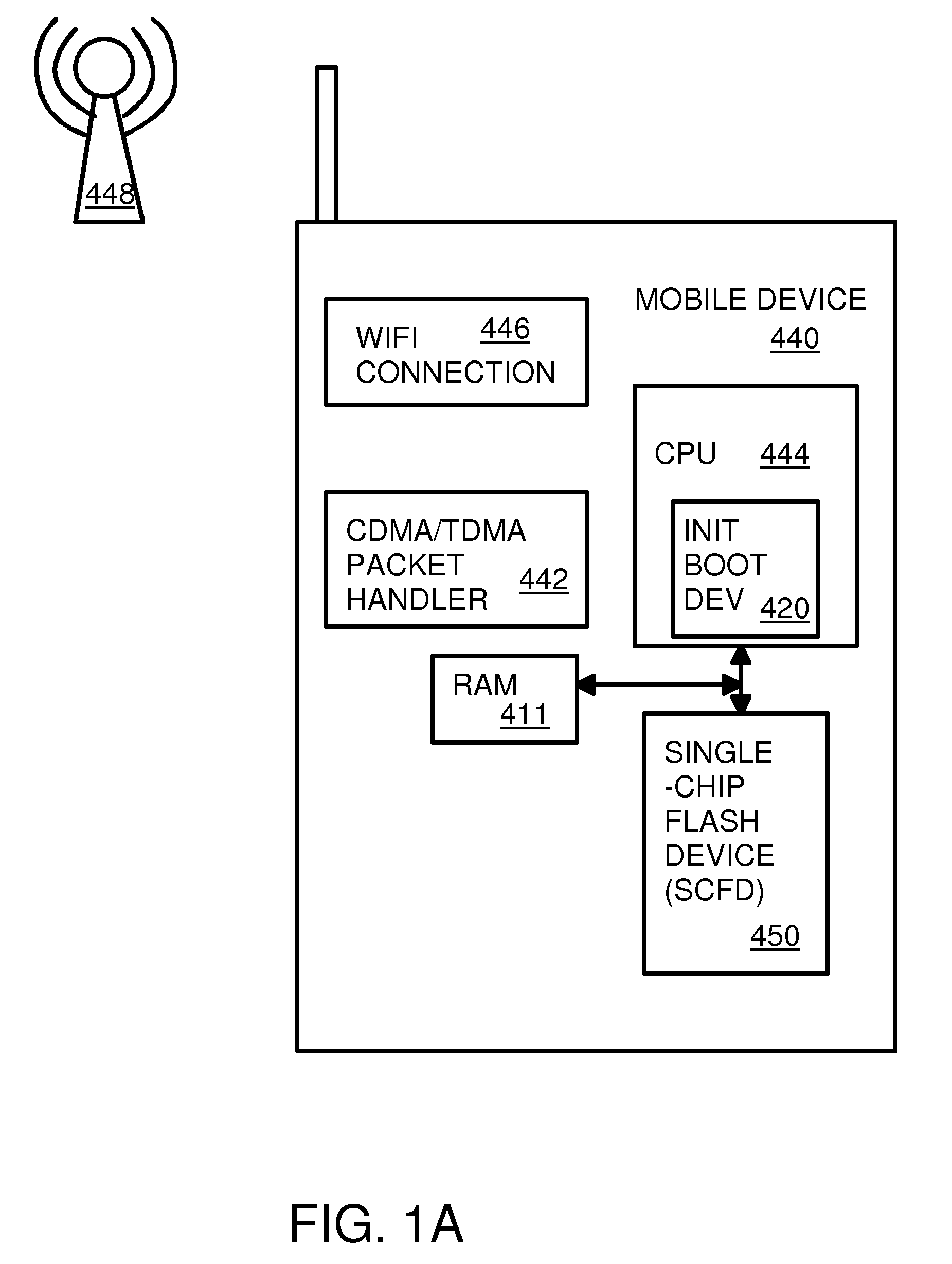
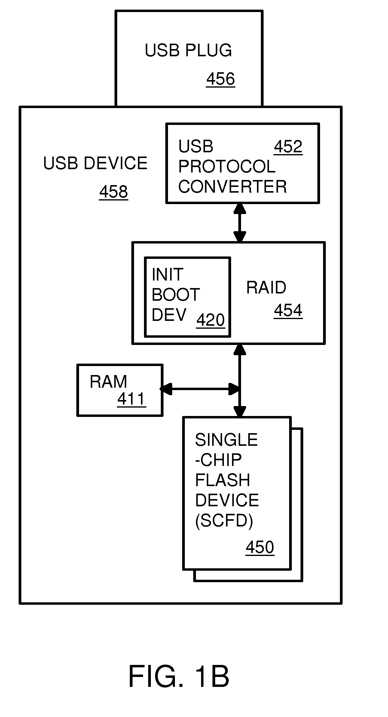
FIG. 1A shows a mobile-device application for a single-chip flash device. Mobile device 440 may be a mobile phone, smart phone, mobile terminal, music player, or combo device. WiFi connection 446 contains a Radio-Frequency (RF) transceiver that wirelessly connects to antenna 448 and to a network such as the Internet. CDMA / TDMA packet h...


PUM


Abstract

A Multi-Media Card (MMC) Single-Chip Flash Device (SCFD) contains a MMC flash microcontroller and flash mass storage blocks containing flash memory arrays that are block-addressable rather than randomly-addressable. An initial boot loader is read from the first page of flash by a state machine and written to a small RAM. A central processing unit (CPU) in the microcontroller reads instructions from the small RAM, executing the initial boot loader, which reads more pages from flash. These pages are buffered by the small RAM and written to a larger DRAM. Once an extended boot sequence is written to DRAM, the CPU toggles a RAM_BASE bit to cause instruction fetching from DRAM. Then the extended boot sequence is executed from DRAM, copying an OS image from flash to DRAM. Boot code and control code are selectively overwritten during a code updating operation to eliminate stocking issues.

Description

FIELD OF THE INVENTIONThis invention relates to flash memory storage, and more particularly to a flash-memory controller integrated with a parallel flash memory.BACKGROUND OF THE INVENTIONFlash memory has gained wide acceptance for its non-volatile storage, which is ideal for portable devices that may lose power, since the data is not lost when stored in the flash memory. Flash memories are constructed from electrically-erasable programmable read-only memory (EEPROM) cells.Rather than use a randomly-addressable scheme such as is common with dynamic-random-access memory (DRAM), many flash memories use a block-based addressing where a command and an address are sent over the data bus and then a block of data is read or written. Since the data bus is also used to send commands and addresses, fewer pins are needed on the flash-memory chip, reducing cost. Thus flash memory is often used as a mass-storage device rather than a randomly-addressable device.Universal-Serial-Bus (USB) has beco...

Claims


Application Information

Patent Timeline
Patent Type & Authority Applications(United States)
IPC IPC(8): G06F15/177G06F12/02G06F13/28G06F9/24
CPCG06F9/4401G06F2213/3854G06F13/387
Inventor LEE, CHARLES C.MA, ABRAHAM C.YU, FRANKCHEN, SHIMON
Owner SUPER TALENT TECH CORP
Learn More