
Method for variable length opcode mapping in a VLIW processor

a variable length opcode and processor technology, applied in the field of processor chips, can solve the problems of inability to add another bit to the signal grouping of instruction, inability to support multiply operation, and waste of program memory by containing nop or vnop, so as to reduce the waste of program memory, reduce program memory, and save program memory.

Inactive Publication Date: 2011-03-24
MIMAR TIBET
View PDF8 Cites 17 Cited by
  • Summary
  • Abstract
  • Description
  • Claims
  • Application Information

AI Technical Summary

Benefits of technology

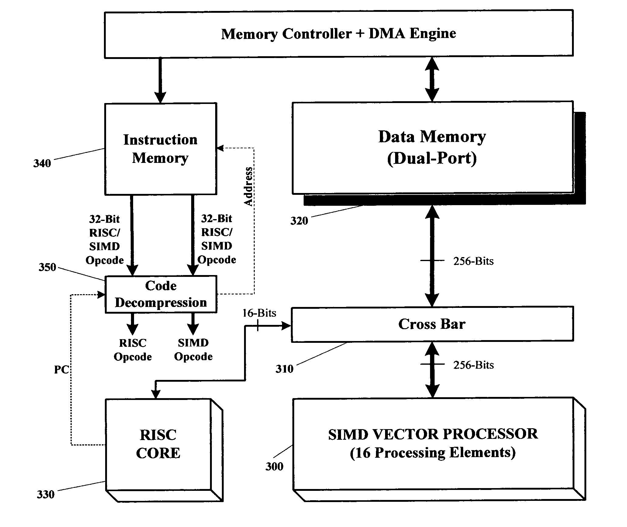
[0010]The present invention provides a method for coding dual-issue opcode fields where first, second, of both opcodes may be active. By coding the map the next 13 instruction pairs in a no-operation instruction provides for supporting of dual-issue and two-instructions sequential execution options. If one opcode is for a scalar processor, and second one is for a SIMD processor, then options of scalar-plus-SIMD, scalar-followed-by-scalar, and SIMD-followed-by-SIMD options are supported in both scalar opcode NOP and SIMD opcode VNOP indicating the map of next 13 instruction pairs. The method of present invention reduces the waste of program memory by compacting opcodes together instead of storing NOP or VNOP instructions, which equals to about 50 percent savings in program memory, or 50 percent reduction in program memory that is required.

Problems solved by technology

The disadvantage of this is that it requires one more bit to code grouping of instructions per opcode, or 8-bits total for 256-wide total combined opcode.
In this case, all instructions could run on each of the execution unit, but with some restrictions, for example, certain execution units do not support multiply operation.
However, this means quite of portion of program memory is wasted by containing NOP or VNOP because typically the ratio of one used to both used is probably about 50 percent.
Adding another bit to signal grouping of instruction would not be feasible because there is usually no space for P-bit within the 32-bit opcode space of either RISC or SIMD.

Method used


Image

  • Method for variable length opcode mapping in a VLIW processor
  • Method for variable length opcode mapping in a VLIW processor
  • Method for variable length opcode mapping in a VLIW processor

Examples


Embodiment Construction

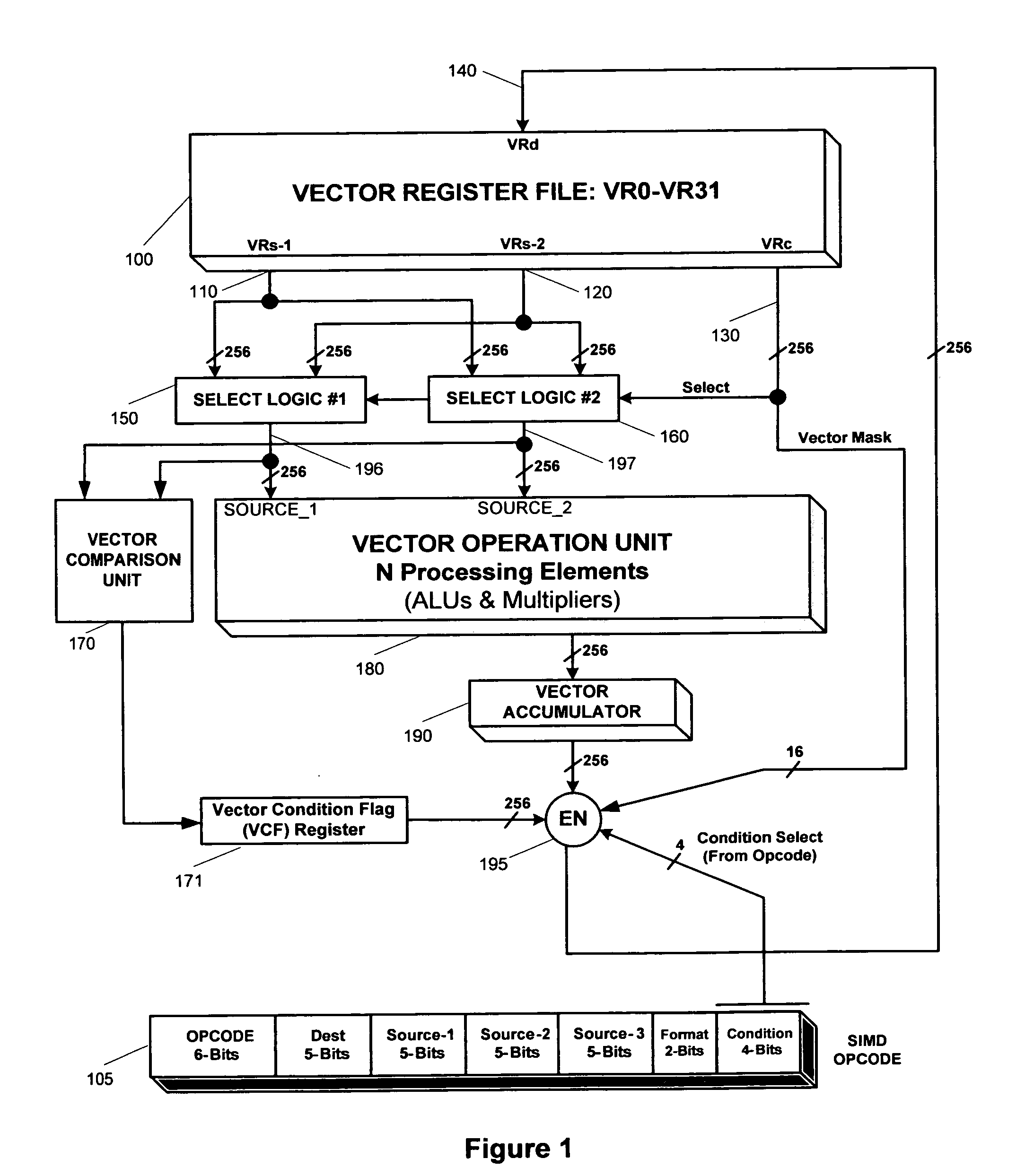
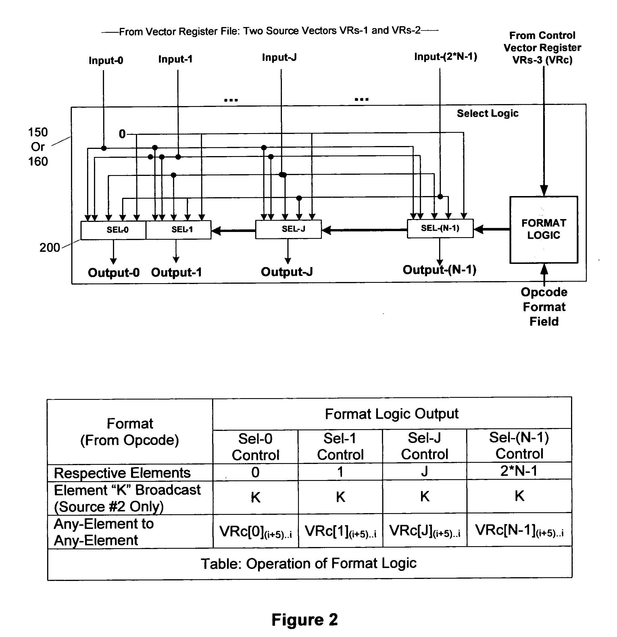
[0027]The SIMD unit consists of a vector register file 100 and a vector operation unit 180, as shown in FIG. 1. The vector operation unit 180 is comprised of plurality of processing elements, where each processing element is comprised of ALU and multiplier. Each processing element has a respective 48-bit wide accumulator register for holding the exact results of multiply, accumulate, and multiply-accumulate operations. These plurality of accumulators for each processing element form a vector accumulator 190. The SIMD unit uses a load-store model, i.e., all vector operations uses operands sourced from vector registers, and the results of these operations are stored back to the register file. For example, the instruction “VMUL VR4, VR0, VR31” multiplies sixteen pairs of corresponding elements from vector registers VR0 and VR31, and stores the results into vector register VR4. The results of the multiplication for each element results in a 32-bit result, which is stored into the accumu...


PUM


Abstract

The present invention provides a method for reducing program memory size required for a dual-issue processor with a scalar processor plus a SIMD vector processor. Coding the map of next group of instruction pairs in a no-operation (NOP) instruction of scalar and vector processor reduces the cases where one of the scalar or vector opcode being a NOP opcode. NOP for either scalar or vector processor defines the next 13 instructions as scalar-plus-vector, scalar-followed-by-scalar, or vector-followed-by-vector so that execution unit performs accordingly until next NOP or a branch instruction.

Description

BACKGROUND OF THE INVENTION[0001]1. Field of the Invention[0002]The invention relates generally to the field of processor chips and specifically to the field of single-instruction multiple-data (SIMD) processors. More particularly, the present invention relates to conditional and nested vector operations in a SIMD processor.[0003]2. Description of the Background Art[0004]Dual-issue processors execute two instructions at the same time. In some systems the execution units and instructions are identical, and either or both instruction could be executed depending on the processing requirements. TI's 8-wide VLIW processor have 8 execution units, and could issue 1 to eight instructions for each cycle [Simar, U.S. Pat. No. 6,182,203]. The execution units are not identical in this case. To signal grouping of instruction to be executed together, the following format is used:[0005]Instruction 1 ∥[0006]Instruction 2 ∥[0007]Instruction 3[0008]Instruction 4 ∥[0009]Instruction 5In this case, inst...

Claims


Application Information

Patent Timeline
IPC IPC(8): G06F15/76G06F9/06
CPCG06F15/8076G06F9/30036G06F9/30072G06F9/30076G06F9/30094G06F9/3887G06F9/30145G06F9/30178G06F9/3822G06F9/3853G06F9/30112
Inventor MIMAR, TIBET
Owner MIMAR TIBET
Learn More