Electrical fuse structure and method for fabricating the same

a technology of electrical fuse and fuse structure, applied in the field of electrical fuse, can solve the problems of defective circuits, fuses can be selectively blown for repair, and the whole chip will be unusable, and achieve the effect of improving the bottleneck of current fuse structur

Inactive Publication Date: 2011-03-31
UNITED MICROELECTRONICS CORP +1
View PDF42 Cites 39 Cited by
  • Summary
  • Abstract
  • Description
  • Claims
  • Application Information

AI Technical Summary

Benefits of technology

The purpose of this invention is to improve upon existing methods of creating electrical fuses by addressing their limitations.

Problems solved by technology

The technical problem addressed in this patent text relates to improving the current capability of electrical fuses while maintaining their reliability at small scales. Conventional methods require large driving devices which limit scaling capabilities. A new solution needs to allow for efficient use of limited resources during fabrication without compromising functionality.

Method used


Image

  • Electrical fuse structure and method for fabricating the same
  • Electrical fuse structure and method for fabricating the same
  • Electrical fuse structure and method for fabricating the same

Examples


Embodiment Construction

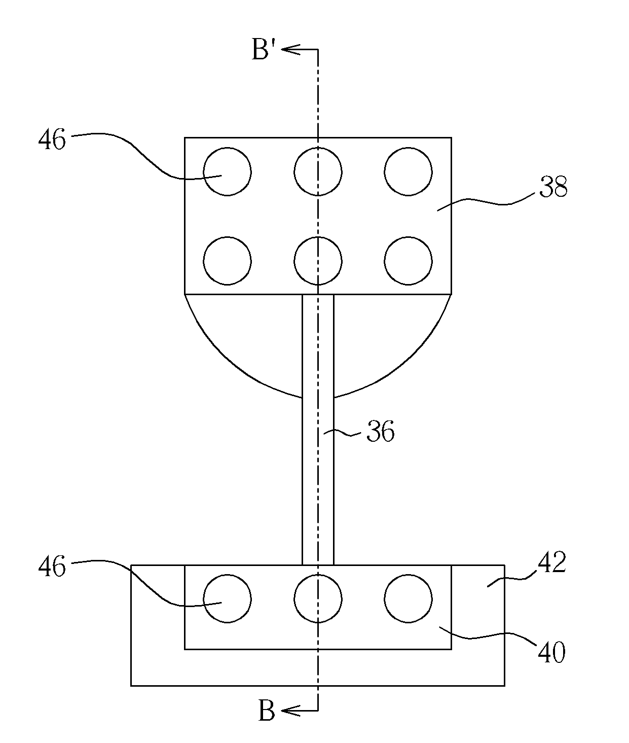
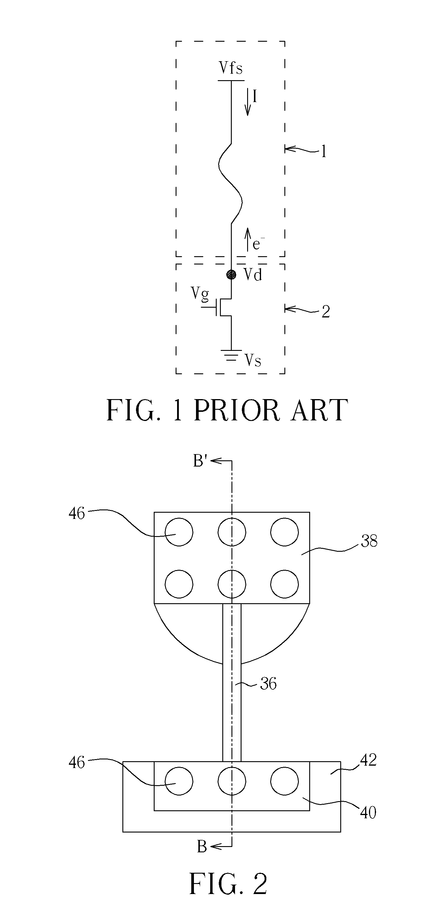
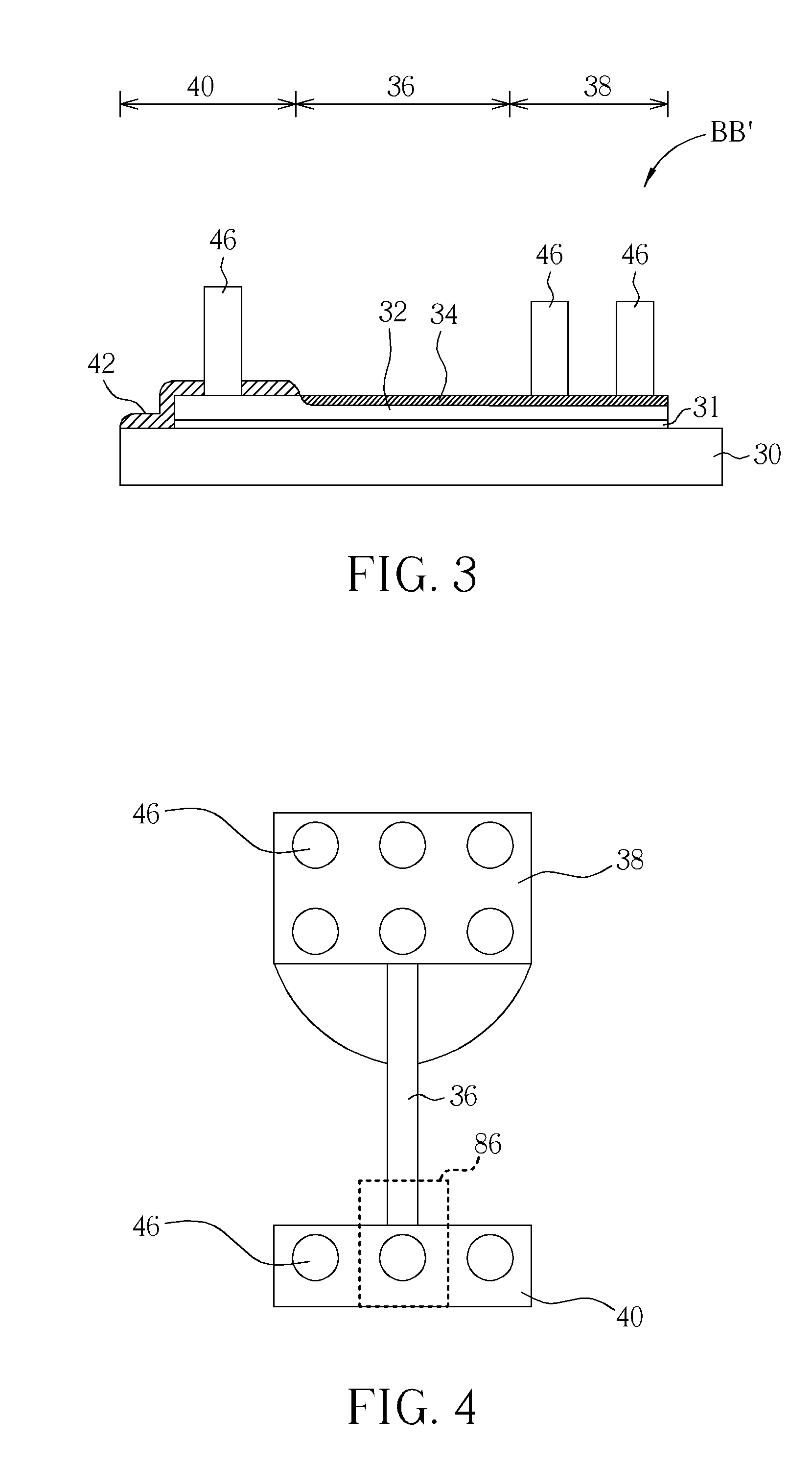
[0018]Referring to FIGS. 2-3, FIG. 2 illustrates a top-view of an electrical fuse structure according to a preferred embodiment of the present invention, and FIG. 3 illustrates a cross-sectional view of FIG. 2 along sectional line BB'. As shown in the figures, a semiconductor substrate 30 is provided, and an insulating layer 31 such as a silicon substrate composed of SiCOH, SiO2 or Si3N4 is formed on the semiconductor substrate 30. A polysilicon layer (not shown) is then deposited on the semiconductor substrate 30, and a pattern transfer is conducted by using patterned photoresist to remove a portion of the polysilicon layer to form a fuse element 36 and an anode 38 and a cathode 40 connected to two ends of the fuse element 36 on the insulating layer 31, in which the fuse element 36, the anode 38, and the cathode 40 are composed of a patterned polysilicon layer 32. In this embodiment, the fuse element 36, the anode 38, and the cathode 40 are preferably composed of polysilicon materi...


PUM

PropertyMeasurementUnit
Widthaaaaaaaaaa

Abstract

An electrical fuse structure is disclosed. The electrical fuse structure includes: a fuse element disposed on surface of a semiconductor substrate; an anode electrically connected to one end of the fuse element; and a cathode electrically connected to another end of the fuse element, wherein no silicide is formed on at least part of the cathode of the electrical fuse structure.

Description


Claims


Application Information

Patent Timeline
Owner UNITED MICROELECTRONICS CORP
Why Eureka
Try Eureka