Embedded chip package process
a chip and embedded technology, applied in the manufacture of printed circuits, printed circuit parts, basic electric elements, etc., can solve the problems of increasing the carrying surface area and not being a good option, and achieve the effect of not increasing the volume of the embedded chip packag
- Summary
- Abstract
- Description
- Claims
- Application Information
AI Technical Summary
Benefits of technology
Problems solved by technology
Method used
Image

Examples
Embodiment Construction
[0020]Reference will now be made in detail to the present preferred embodiments of the invention, examples of which are illustrated in the accompanying drawings. Wherever possible, the same reference numbers are used in the drawings and the description to refer to the same or like parts.
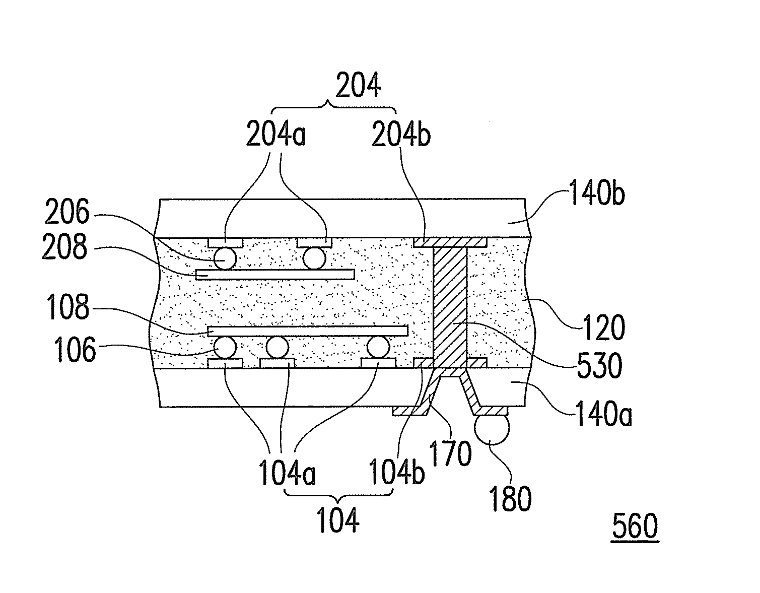
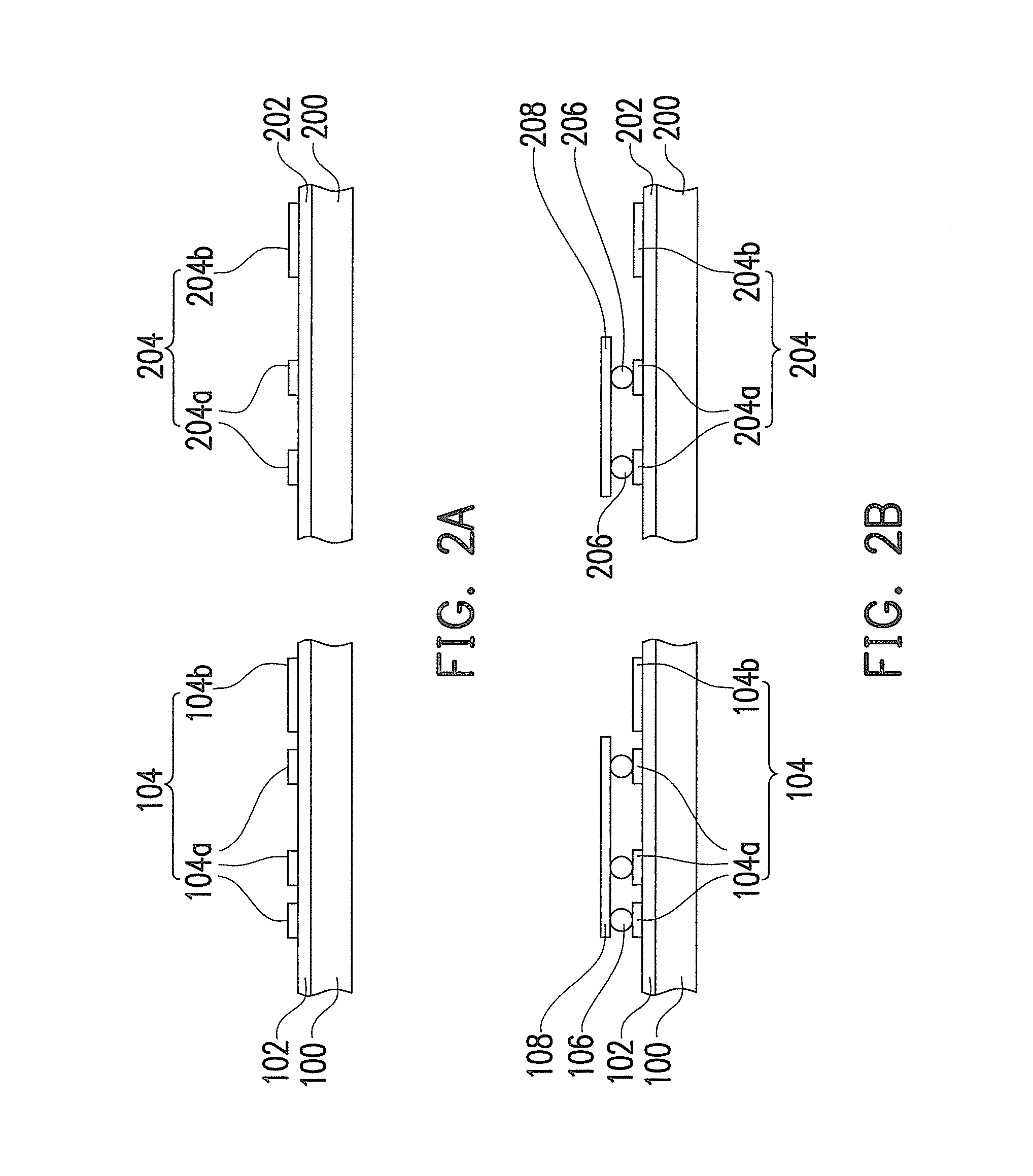
[0021]FIGS. 2A through 2E are schematic cross-sectional views showing the steps in an embedded chip package process according to one embodiment of the present invention. As shown in FIG. 2A, a first substrate 100 and a second substrate 200 are provided. The first substrate 100 has a first adhesion layer 102 and a first patterned circuit layer 104 thereon, and the second substrate 200 has a second adhesion layer 202 and a second patterned circuit layer 204 thereon. The first patterned circuit layer 104 is disposed on the first adhesion layer 102 and has a plurality of bonding pads 104a and at least a first contact 104b. The second patterned circuit layer 204 is disposed on the second adhesion layer 20...
PUM
 Abstract
Description
Claims
Application Information
 - R&D
- Intellectual Property
- Life Sciences
- Materials
- Tech Scout
- Unparalleled Data Quality
- Higher Quality Content
- 60% Fewer Hallucinations
Browse by: Latest US Patents, China's latest patents, Technical Efficacy Thesaurus, Application Domain, Technology Topic, Popular Technical Reports.
© 2025 PatSnap. All rights reserved.Legal|Privacy policy|Modern Slavery Act Transparency Statement|Sitemap|About US| Contact US: help@patsnap.com