Semiconductor package, semiconductor package structure including the semiconductor package, and mobile phone including the semiconductor package structure

a semiconductor package and semiconductor technology, applied in the direction of semiconductor/solid-state device details, semiconductor devices, electrical devices, etc., can solve the problems of increasing the manufacturing cost of the semiconductor package structure, the side of the semiconductor chip may not be physically supported from adjacent semiconductor chips of the part, and the filling structure may not sufficiently fill the concave portion of the semiconductor chip

Active Publication Date: 2011-04-07
SAMSUNG ELECTRONICS CO LTD
View PDF18 Cites 30 Cited by
  • Summary
  • Abstract
  • Description
  • Claims
  • Application Information

AI Technical Summary

Benefits of technology

[0010]Example embodiments provide a semiconductor package in which concave portions around semiconductor chips may be sufficiently filled when the semiconductor chips have cascade shapes at both sides thereof.
[0011]Example embodiments also provide a semiconductor package structure capable of preventing cracks from occurring at least one side of semiconductor chips which form cascade shapes.

Problems solved by technology

In this case, the filling structure may not sufficiently fill the concave portion of the semiconductor chips.
A change in the filling structure may increase a manufacturing cost of the semiconductor package structure.
Besides, sides of the part of the semiconductor chips may not be physically supported from adjacent semiconductor chips of the part.
In this case, the pressure of the unit for supplying the conductive material may cause cracks in the sides of the part of the semiconductor chips.
The cracks in the semiconductor chips may deteriorate physical characteristics and / or electrical characteristics of the semiconductor package structure.
The processor-based systems and / or mobile phones may not sufficiently store desired data in the semiconductor package structure due to voids and / or cracks in the semiconductor package structure.

Method used


Image

  • Semiconductor package, semiconductor package structure including the semiconductor package, and mobile phone including the semiconductor package structure
  • Semiconductor package, semiconductor package structure including the semiconductor package, and mobile phone including the semiconductor package structure
  • Semiconductor package, semiconductor package structure including the semiconductor package, and mobile phone including the semiconductor package structure

Examples


Embodiment Construction

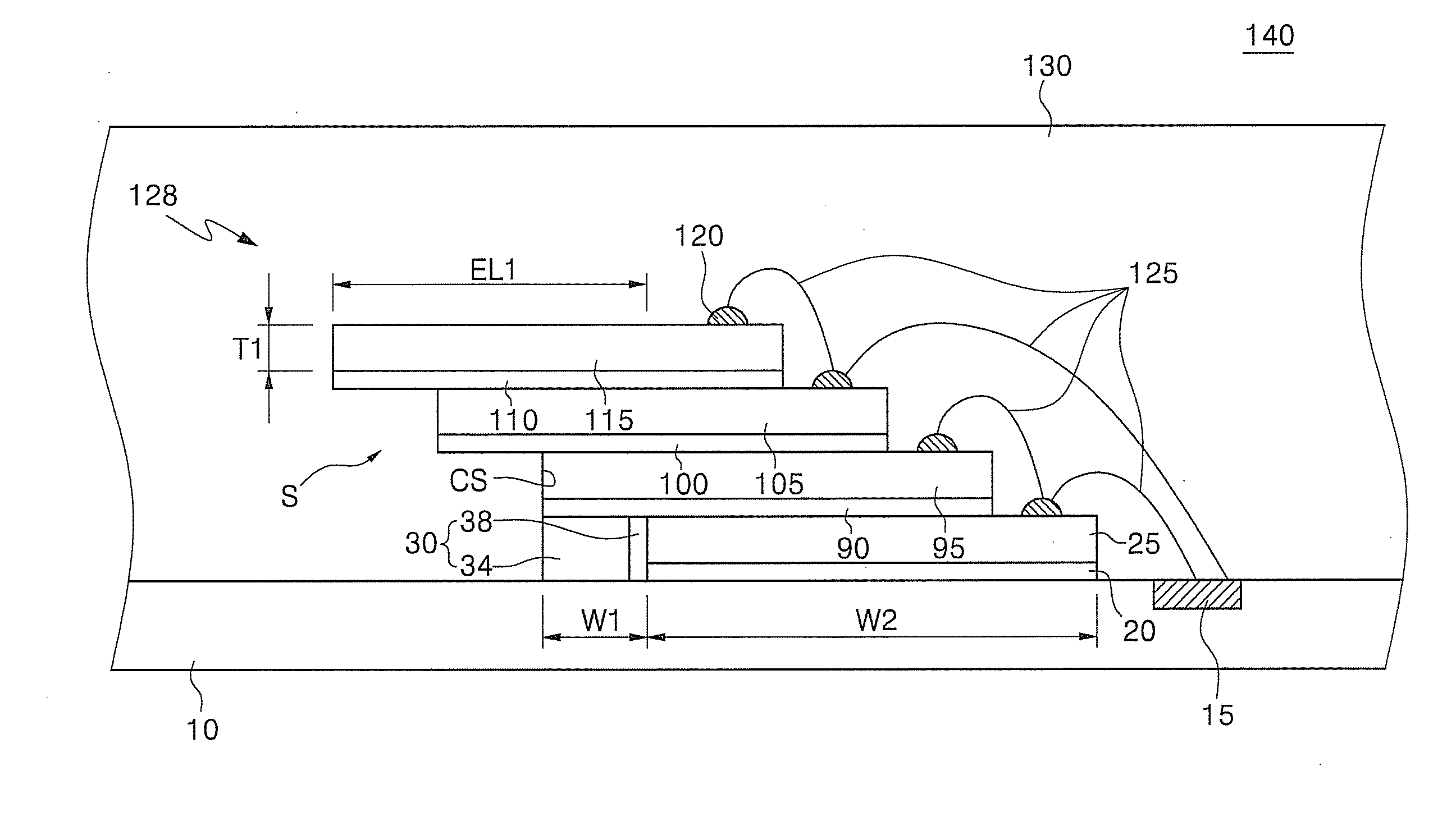
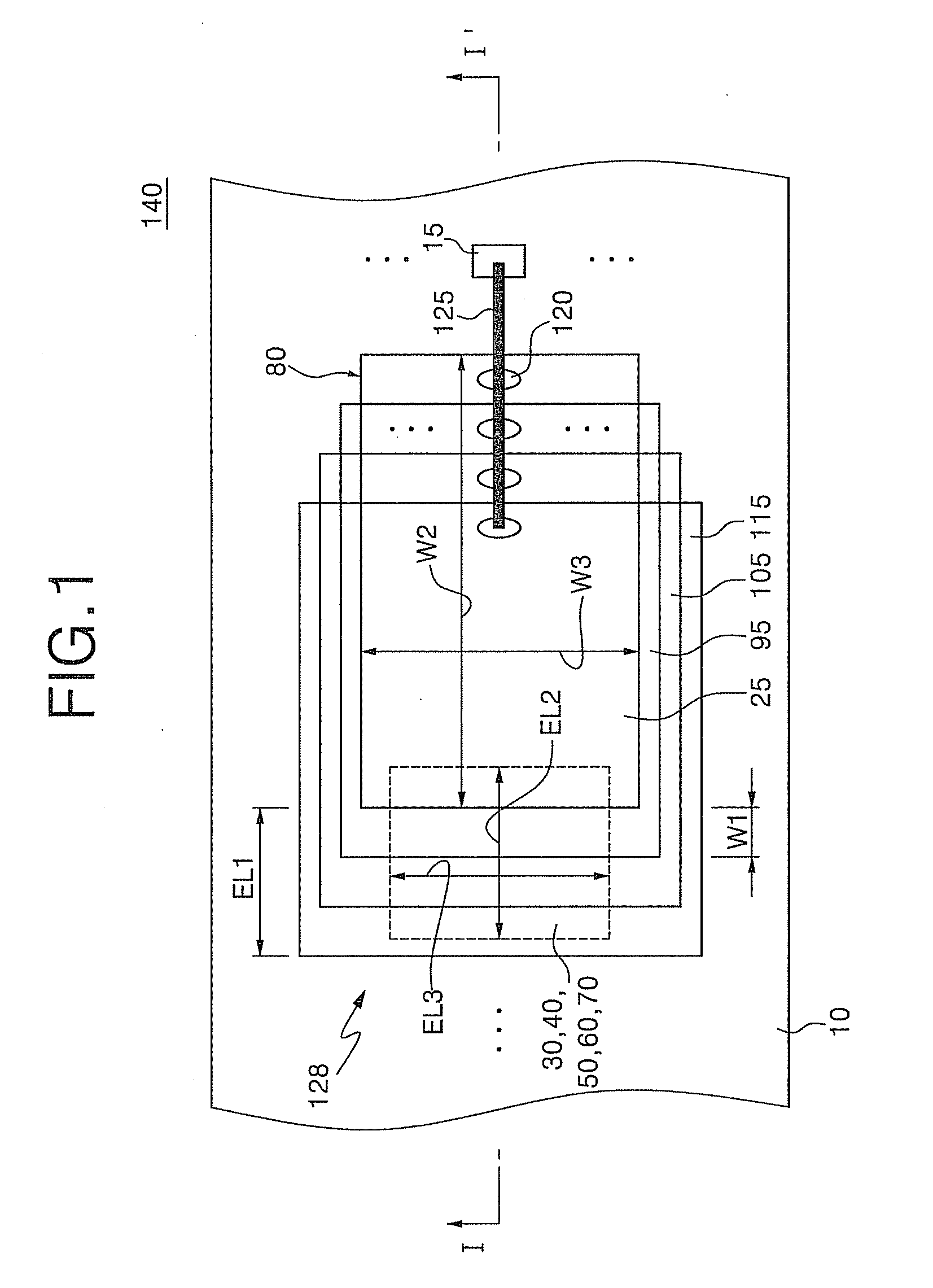
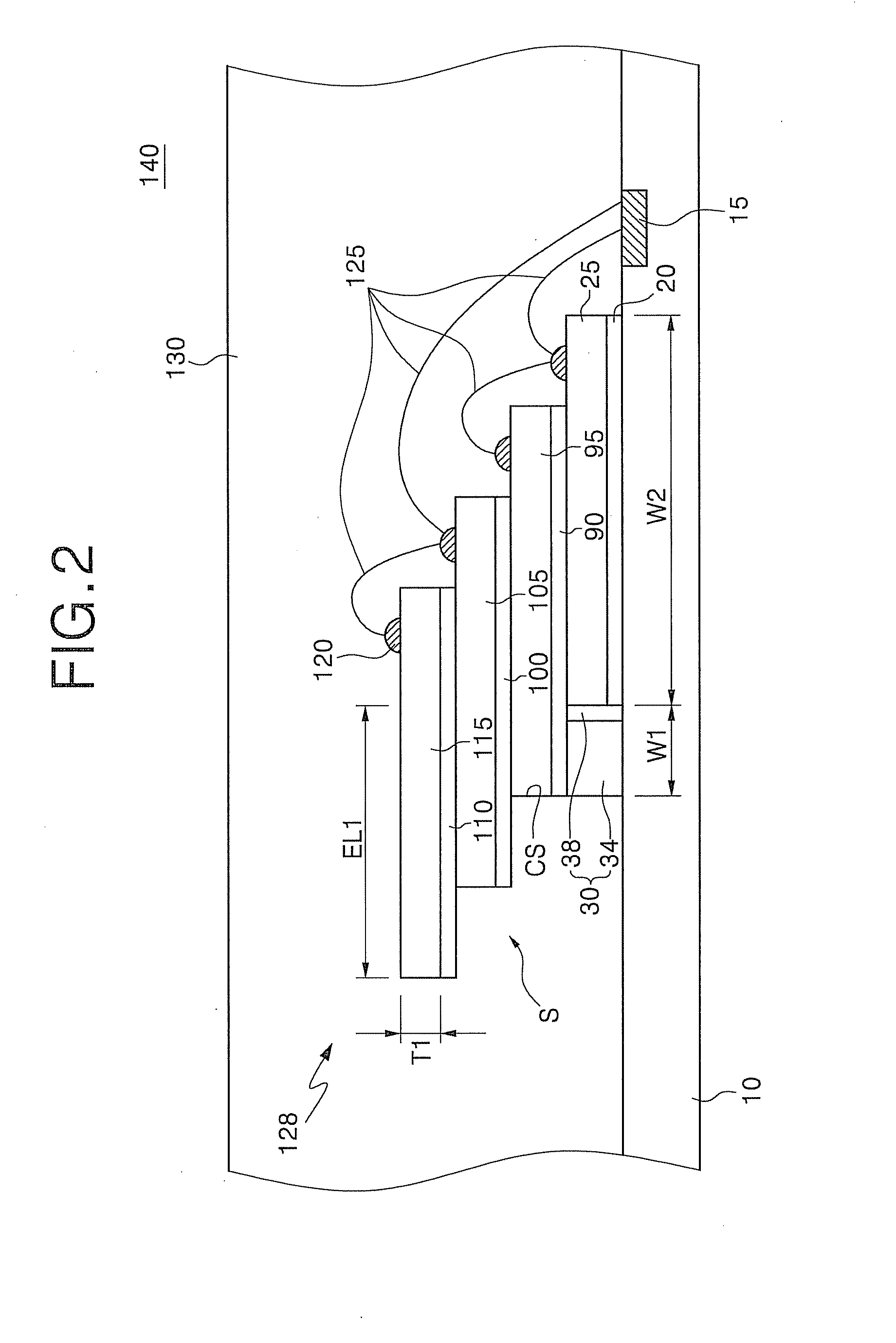
[0053]Example embodiments will now be described more fully with reference to the accompanying drawings in which example embodiments are shown. Example embodiments may, however, be embodied in different forms and should not be construed as limited to example embodiments set forth herein. Rather, example embodiments are provided so that this disclosure is thorough and complete and fully conveys the inventive concepts to those skilled in the art. In the drawings, the sizes and relative sizes of layers and regions may be exaggerated for clarity.

[0054]It will be understood that when an element or layer is referred to as being “on,”“connected to” or “coupled to” another element or layer, it can be directly on, connected or coupled to the other element or layer or intervening elements or layers may be present. In contrast, when an element is referred to as being “directly on,”“directly connected to” or “directly coupled to” another element or layer, there are no intervening elements or lay...


PUM


Abstract

Provided is a semiconductor package. The semiconductor package may include a first semiconductor package having first semiconductor chips sequentially stacked on a substrate. In example embodiments, the first semiconductor chips may have a cascaded arrangement in which first sides and second sides of the semiconductor chips define cascade patterns. The cascaded arrangement may extend in a first direction to define a space between the first sides of the first semiconductor chips and the substrate. The semiconductor package may also include at least one first connection wiring at the second sides of the semiconductor chips, the at least one first connection wiring being configured to electrically connect the substrate with the first semiconductor chips. In addition, the semiconductor package may further include a first filling auxiliary structure adjacent to the first sides of the first semiconductor chips.

Description

CROSS-REFERENCE TO RELATED APPLICATION[0001]This application claims priority under 35 U.S.C. §119 to Korean Patent Application No. 10-2009-0094832, filed on Oct. 6, 2009, in the Korean Intellectual Property Office (KIPO) and Korean Patent Application No. 10-2010-0036505, filed on Apr. 20, 2010, in the Korean Intellectual Property Office (KIPO), the contents of each are hereby incorporated by reference in their entirety.BACKGROUND[0002]1. Field[0003]Example embodiments relate to a semiconductor package, a semiconductor package structure including the semiconductor package, and a mobile phone including the semiconductor package structure.[0004]2. Description of Related Art[0005]In recent years, a semiconductor package structure has come to include semiconductor chips which are sequentially stacked on a substrate for high integration. The semiconductor chips have become thinner and thinner in thickness in response to a trend toward the high integration. The semiconductor chips may be d...

Claims


Application Information

Patent Timeline
Patent Type & Authority Applications(United States)
IPC IPC(8): H01L25/04
CPCH01L23/16H01L2924/12041H01L23/481H01L24/05H01L24/29H01L24/32H01L24/33H01L24/48H01L24/49H01L24/83H01L25/0657H01L25/50H01L2224/04042H01L2224/05556H01L2224/05599H01L2224/32145H01L2224/32225H01L2224/48091H01L2224/48145H01L2224/48147H01L2224/48227H01L2224/48465H01L2224/49111H01L2224/49175H01L2224/73265H01L2224/83191H01L2224/838H01L2224/85399H01L2224/92H01L2224/92247H01L2225/06506H01L2225/0651H01L2225/06541H01L2225/06562H01L2924/01014H01L2924/078H01L2924/10158H01L2924/14H01L2924/1433H01L2924/00014H01L2924/01005H01L2924/01006H01L2924/01033H01L2924/01055H01L23/3121H01L2224/45099H01L2924/00H01L2924/3512H01L2924/00012H01L2924/181H01L24/73
Inventor SONG, IN-SANGLIM, SEOK-KEUNJUNG, IN-WOOKYU, BONG-KENPARK, SANG-WOOKHONG, JI-SEOK
Owner SAMSUNG ELECTRONICS CO LTD
Why Eureka
Try Eureka