

Image taking device and camera system
Active Publication Date: 2011-04-07
SONY SEMICON SOLUTIONS CORP
View PDF3 Cites 78 Cited by
- Summary
- Abstract
- Description
- Claims
- Application Information
AI Technical Summary
Benefits of technology
[0033]In accordance with embodiments of the present invention, it is possible to carry out a light-quantity measurement process and an image taking process at a large dynamic range without reducing the pixel aperture ratio by processing no analog signals and by generating only few noises even at a low illumination intensity.
Problems solved by technology
On the other side of the coin, however, a system employing the photon counter is expensive and the dynamic range of a measurement process is narrow.
However, the image taking process as described above raises problems.
One of the problems is noises generated in propagation of the analog signal.
Another problem is the speed of the AD converter.
Thus, the size of a system for AD conversion is very large.
However, there is no device that meets both of these requirements.
By making use of an ordinary photon counter, however, a dynamic range sufficient for the image taking operation is not satisfied.
However, such a system is extremely expensive.
In accordance with the technology disclosed in Patent Document 1, however, every pixel requires a sense circuit and a counter so that the aperture area of the pixel inevitably becomes very small.
Thus, the circuit size of a chip including the counters is unavoidably large.
Method used
View moreImage
Smart ImageViewing Examples

Examples
first embodiment (
2. First embodiment (first configuration of the image taking device)
second embodiment (
3. Second embodiment (second configuration of the image taking device)
third embodiment (
4. Third embodiment (exemplary application of the image taking device)
Login to View More PUM
 Abstract
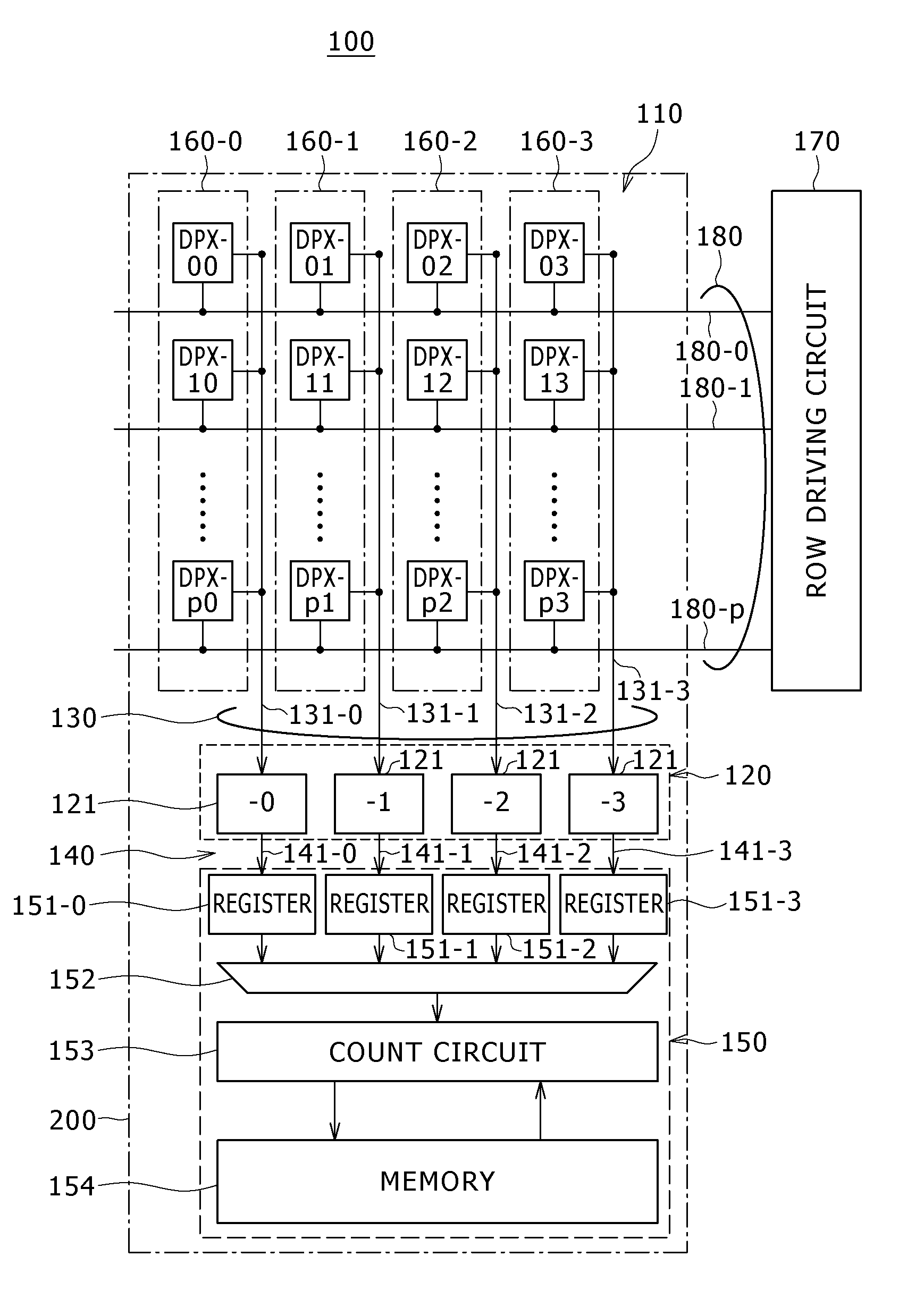
An image sensor includes a plurality of pixels, a plurality of sense circuits, and a count circuit. Each sense circuit is configured to read out electrical signals from at least one pixel associated with the sense circuit in order to generate data representing whether or not photons have been received by the sense circuit. The count circuit is in communication with a sense circuit selected from the plurality of sense circuits. The count circuit is configured to provide integration results for the pixels associated with the sense circuits based on the data received from the sense circuits.
Description
RELATED APPLICATION DATA[0001]The present application claims priority to Japanese Priority Patent Application JP 2009-229893 filed in the Japan Patent Office on Oct. 1, 2009, which is incorporated by reference in its entirety to the extent permitted by law.BACKGROUND OF THE INVENTION[0002]The present invention relates to image taking devices such as a CMOS (Complementary Metal Oxide Semiconductor) image sensors and camera systems employing same.[0003]In recent years, techniques for measuring minute amounts of light emitted by or from a biological body and fluorescent light, as well as techniques for taking images, have been developed in the fields of medical cares and biotechnologies.[0004]In addition, a transmission image taking technology has been applied to products in the medical-care and security fields. In accordance with the transmission image taking technology, few X rays passing through an object of observation are converted by a scintillator into photons at the visible lev...
Claims
Login to View More Application Information
Patent Timeline
 IPC IPC(8): H04N5/335
CPCH04N5/32H04N5/357H04N5/355H04N5/3355H04N25/772H04N25/57H04N25/00H04N25/60H04N25/65H04N25/75H04N25/533H04N25/767G01J1/44G01J2001/444
InventorNISHIHARA, TOSHIYUKI
OwnerSONY SEMICON SOLUTIONS CORP