Multichamber split processes for LED manufacturing

a technology of led manufacturing and multi-chamber split, which is applied in the field of manufacturing of devices, can solve problems such as the reduction of electroluminescen

Inactive Publication Date: 2011-04-07
APPLIED MATERIALS INC
View PDF38 Cites 28 Cited by
  • Summary
  • Abstract
  • Description
  • Claims
  • Application Information

AI Technical Summary

Problems solved by technology

However, the growth interruption experienced during transfer between chambers may lead to reduction of electroluminescence.

Method used


Image

  • Multichamber split processes for LED manufacturing
  • Multichamber split processes for LED manufacturing
  • Multichamber split processes for LED manufacturing

Examples


example

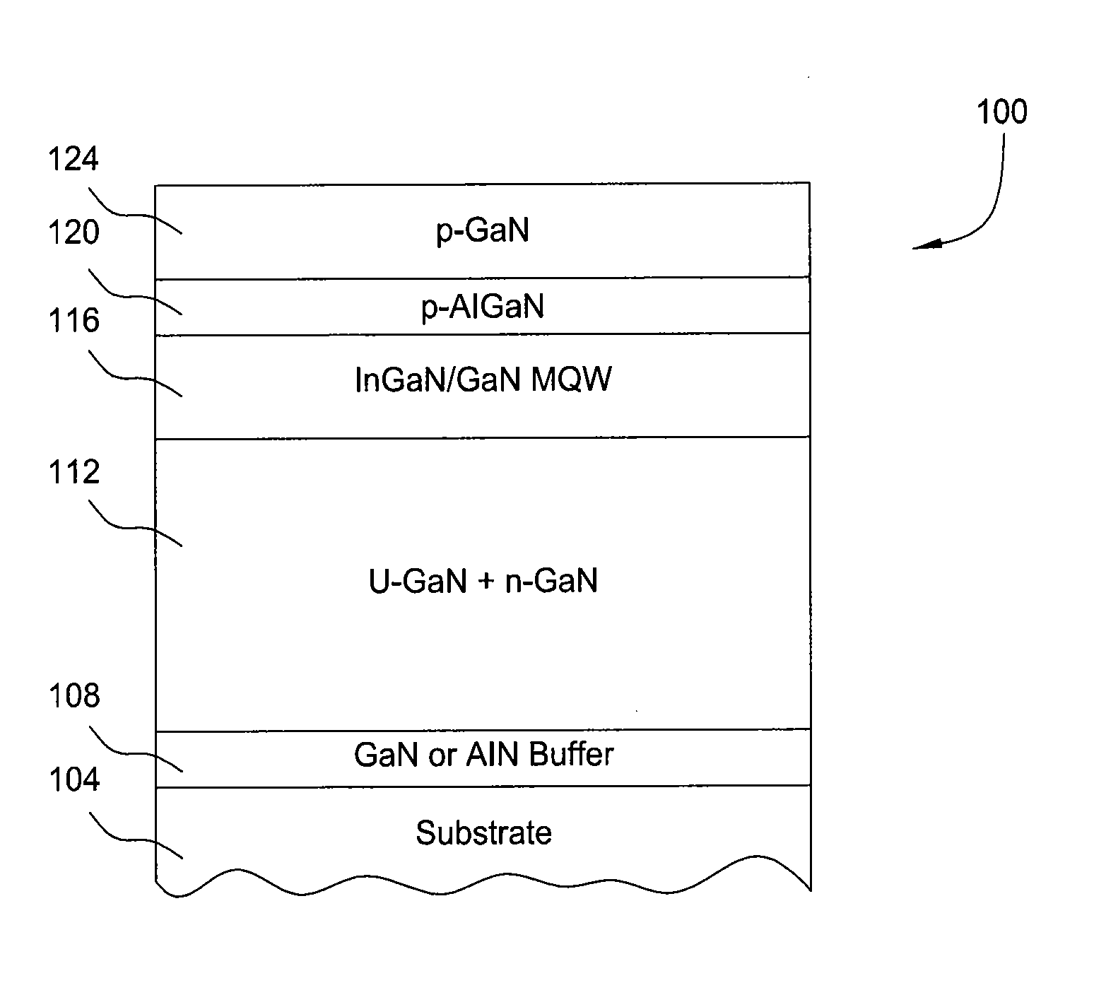
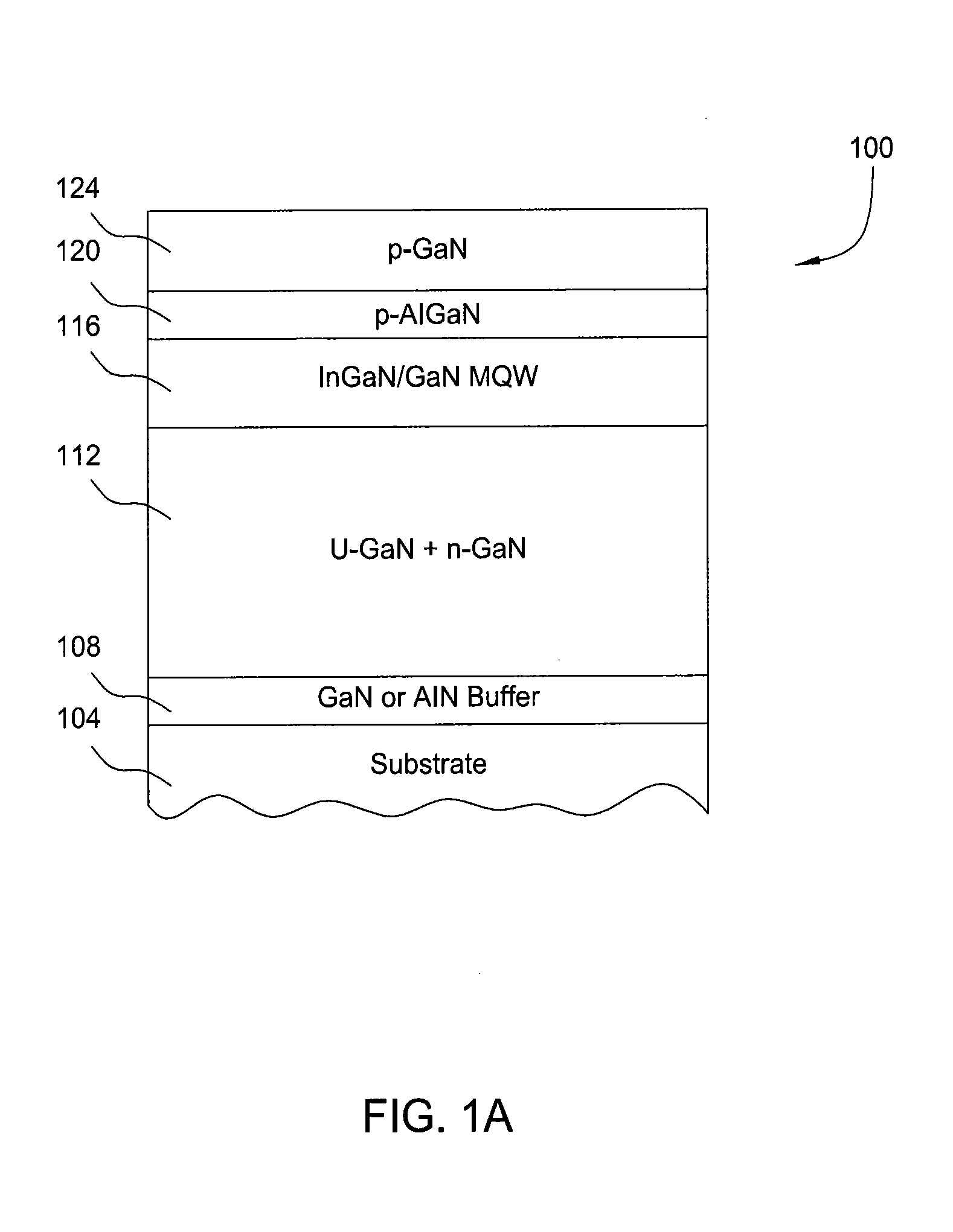
[0065]The following example is provided to illustrate how the general process may be used for the fabrication of compound nitride structures described in connection with processing system 200. The example refers to a LED structure, with its fabrication being performed using a processing system 200 having three MOCVD chambers 202. An overview of the process is provided with the flow diagram of FIG. 6 showing a process sequence 600. The deposition of the initial III1-N layers (e.g., the GaN layers) is performed either in the first MOCVD chamber 202a or the HVPE chamber 204, deposition of III2-N layers (e.g., the InGaN layer) is performed in the second MOCVD chamber 202b, and deposition of the III3-N layers (e.g. the AlGaN, and GaN contact layers) is performed in the third MOCVD chamber 202c.

[0066]At block 602 one or more sapphire substrates are transferred into the first substrate processing chamber. Where the first substrate processing chamber is an MOCVD chamber, a carrier plate 31...


PUM

PropertyMeasurementUnit
temperatureaaaaaaaaaa
thicknessaaaaaaaaaa

Abstract

Embodiments described herein generally relate to methods for forming Group III-V materials by metal-organic chemical vapor deposition (MOCVD) processes and / or hydride vapor phase epitaxial (HVPE) processes. In one embodiment, deposition of a group III1-N layer on a substrate is performed in a first chamber, deposition of a group III2-N layer on the substrate is performed in a second chamber, and deposition of a group III3-N layer on the substrate is performed in a chamber different from the chamber where the group III2-N layer is deposited. Between the group III2-N layer deposition and the group III3-N layer deposition, one or more surface treatment processes are performed on the substrate to reduce non-radiative recombination at the interface and improve overall electroluminescence of the produced structure.

Description

CROSS-REFERENCE TO RELATED APPLICATIONS[0001]This application claims benefit of U.S. Provisional Patent Application Ser. No. 61 / 249,470 (APPM / 014457L), filed Oct. 7, 2009, which is herein incorporated by reference.BACKGROUND OF THE INVENTION[0002]1. Field of the Invention[0003]Embodiments of the present invention generally relate to the manufacturing of devices, such as light emitting diodes (LEDs), laser diodes (LDs) and, more particularly, to processes for forming Group III-V materials by metal-organic chemical vapor deposition (MOCVD) and hydride vapor phase epitaxial (HVPE) deposition processes.[0004]2. Description of the Related Art[0005]Group III-V films are finding greater importance in the development and fabrication of a variety of semiconductor devices, such as short wavelength LEDs, LDs, and electronic devices including high power, high frequency, high temperature transistors and integrated circuits. For example, short wavelength (e.g., blue / green to ultraviolet) LEDs are...

Claims


Application Information

Patent Timeline
Patent Type & Authority Applications(United States)
IPC IPC(8): H01L21/20
CPCC23C16/301H01L33/007C23C16/452C23C16/45565C23C16/4557C23C16/45574C23C16/46C23C16/481C23C16/54H01L21/02381H01L21/0242H01L21/02458H01L21/02502H01L21/02505H01L21/0254H01L21/02573H01L21/0262H01L21/67115H01L21/67207C23C16/4481H01L33/02H01L33/32
Inventor SU, JIE
Owner APPLIED MATERIALS INC
Why Eureka
Try Eureka