ALD of metal silicate films

a metal silicate film and siosub>2 technology, applied in the field of metal silicate films, can solve the problems of unreliable thin film, adversely affecting device performance, and difficult to obtain traditional methods full film coverage on deep bottoms and vias

Active Publication Date: 2008-01-24
ASM IP HLDG BV
View PDF43 Cites 335 Cited by
  • Summary
  • Abstract
  • Description
  • Claims
  • Application Information

AI Technical Summary

Benefits of technology

[0014]In other embodiments, hafnium silicate films are provided. The hafnium silicate films preferably comprise carbon impurity concentrations of less than or equal to about 50,000 parts-per-million (ppm) and halogen impurity concentrations of less than or equal to about 20,000 ppm. In some embodiments, the hafnium silicate films have step coverages greater than or equal to about 85%.
[0015]All o

Problems solved by technology

Design rules are setting the feature sizes to ≦0.2 μm, making complete film coverage on deep bottoms and vias difficult to obtain using traditional methods.
Additionally, with decreasing feature sizes, quantum mechanical tunneling (“tunneling”) leads to leakage current, i.e., current leaking out of device features (e.g., across gate oxides), which adversely affects device performance.
For this reason, substantially thin SiO2 films are unreliable as gate dielectrics (gate oxides), for example, in MOSFET (metal-oxide-semiconductor field-effect transistor) devices.
However, with decreasing features sizes, it has become increasingly difficult to deposit hafnium silicate films with compositional and thickness uniformities suited for current and future generat

Method used


Image

  • ALD of metal silicate films
  • ALD of metal silicate films

Examples


example 1

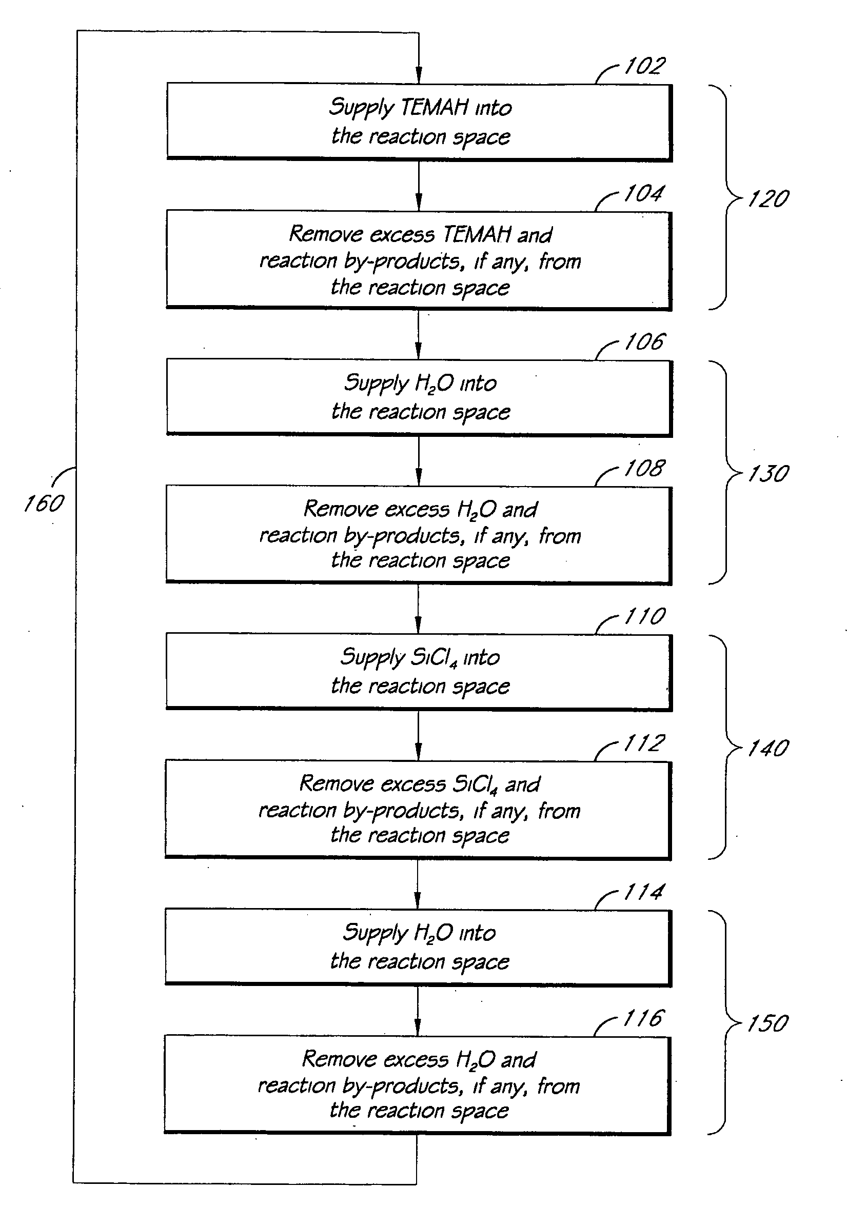
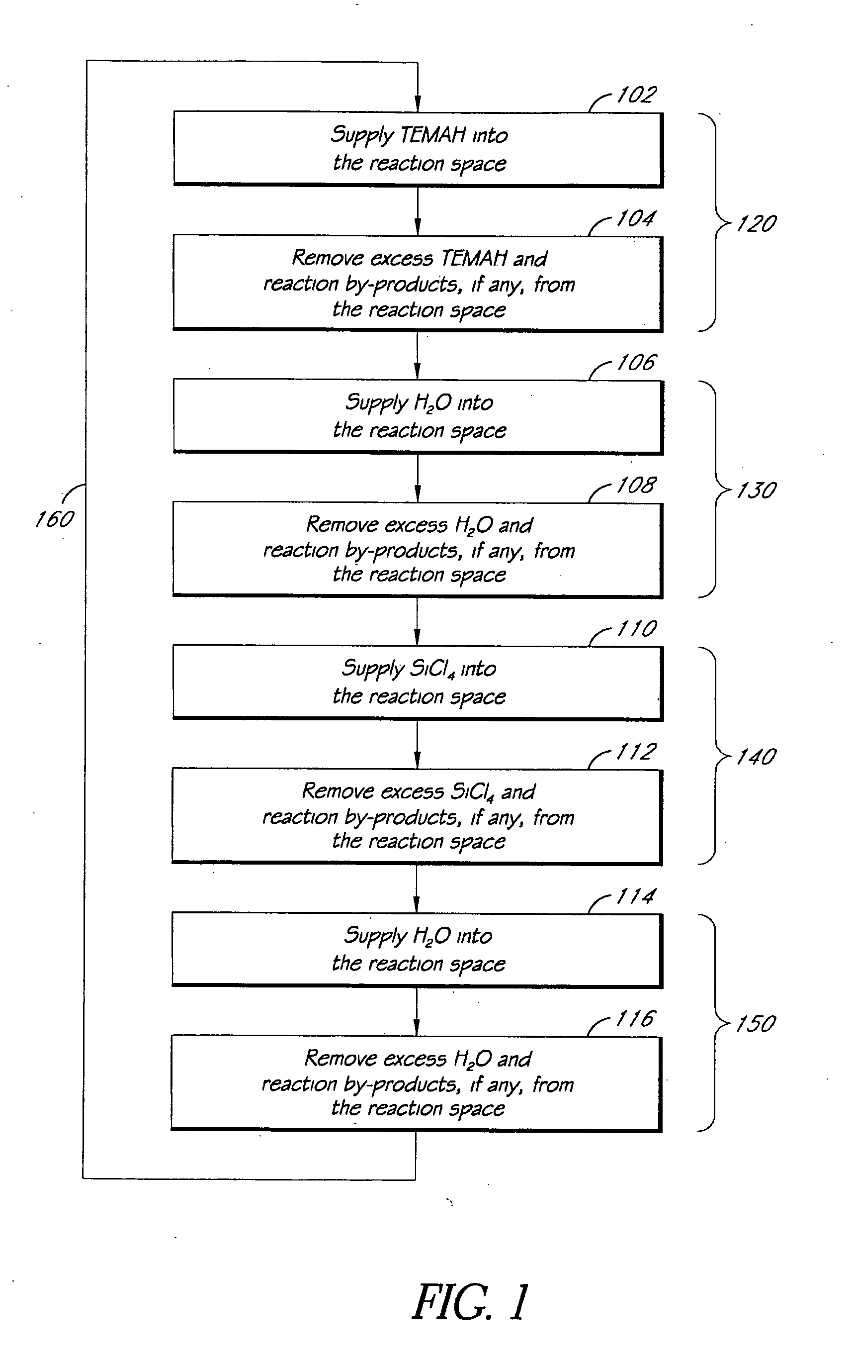
[0080]A hafnium silicate film was deposited on a 300 mm silicon wafer using a Pulsar™ reactor manufactured by ASM America, Inc. The wafer included trenches with depth-to-width aspect ratios greater than about 50:1. Deposition was conducted at a substrate temperature in the range of about 250 to 320° C. The sequence processing steps included the following:

[0081](1) TEMAH pulse;

[0082](2) Ar purge;

[0083](3) H2O pulse;

[0084](4) Ar purge;

[0085](5) SiCl4 pulse;

[0086](6) Ar purge;

[0087](7) H2O pulse; and

[0088](8) Ar purge.

[0089]Steps (1)-(8) were repeated until a hafnium silicate film with a thickness of about 34 Å was formed on the silicon wafer. Uniform coverage was achieved within the trenches. A step coverage in excess of 95% was achieved. The film had a uniformity (1 sigma) of about 0.78%.

example 2

[0090]A hafnium silicate film was grown on a 300 mm silicon wafer at a wafer temperature of about 300° C. TEMAH was used as the metal reactant, SiCl4 was used as the silicon reactant and water was used as the oxidizing agent. The pulsing sequence was TEMAH / H2O / SiCl4 / H2O. The reaction space was purged with Ar between each of said pulses. Each cycle included a TEMAH / H2O pulsing sequence followed by five SiCl4 / H2O pulsing sequences (i.e., Hf / Si pulse ratio was 1:5). The growth rate of the hafnium silicate film was about 0.95 Å / cycle.

[0091]The hafnium silicate film formed had a hafnium concentration of about 18%, a silicon concentration of about 15% and an oxygen concentration of about 66%. Carbon and chlorine impurity levels were less than about 1% (i.e., 10,000 ppm) and 0.2% (i.e., 2000 ppm), respectively, as determined by nuclear reaction analysis (NRA) and rutherford backscattering spectrometry (RBS). The hafnium silicate film had a step coverage of about 100%.

[0092]In at least some...


PUM

PropertyMeasurementUnit
Temperatureaaaaaaaaaa

Abstract

Methods for forming metal silicate films are provided. The methods comprise contacting a substrate with alternating and sequential vapor phase pulses of a metal source chemical, a silicon source chemical and an oxidizing agent. In preferred embodiments, an alkyl amide metal compound and a silicon halide compound are used. Methods according to preferred embodiments can be used to form hafnium silicate and zirconium silicate films with substantially uniform film coverages on substrate surfaces comprising high aspect ratio features (e.g., vias and/or trenches).

Description

REFERENCE TO RELATED APPLICATIONS[0001]The present application is related to U.S. patent application Ser. No. 10 / 148,525 to Tois et al., filed May 31, 2002, and U.S. patent application Ser. No. 10 / 678,766 to Tois et al., filed Oct. 3, 2003, which are entirely incorporated by reference herein.BACKGROUND OF THE INVENTION[0002]1. Field of the Invention[0003]The present invention relates to metal silicate films. In particular, the invention concerns methods for forming metal silicate films by atomic layer deposition (ALD).[0004]2. Description of the Related Art[0005]The integration level of components in integrated circuits is increasing, which rapidly places a demand for a decrease of the size of integrated circuit (IC) components and interconnects. Design rules are setting the feature sizes to ≦0.2 μm, making complete film coverage on deep bottoms and vias difficult to obtain using traditional methods. Additionally, with decreasing feature sizes, quantum mechanical tunneling (“tunneli...

Claims


Application Information

Patent Timeline
IPC IPC(8): H01L21/31
CPCC23C16/401C23C16/405C23C16/45531H01L21/31645H01L21/3141H01L21/31612C23C16/45542H01L21/28194H01L21/02148H01L21/0228H01L21/02159H01L21/31H01L21/20
Inventor WANG, CHANG-GONGSHERO, ERIC J.WILK, GLENMAES, JAN WILLEM
Owner ASM IP HLDG BV
Why Eureka
Try Eureka