
Graphene device and method of manufacturing the same

a graphene device and graphene technology, applied in the direction of semiconductor devices, pulse techniques, electric pulse generator details, etc., can solve the problems of graphene properties changing, operation voltage of fet may increase, and the coupling between the oxide layer and the global back gate may be relatively low, so as to facilitate operation control

Active Publication Date: 2011-04-21
SAMSUNG ELECTRONICS CO LTD
View PDF11 Cites 23 Cited by
  • Summary
  • Abstract
  • Description
  • Claims
  • Application Information

AI Technical Summary

Benefits of technology

[0007]Example embodiments provide a graphene device that may be manufactured using a relatively simple process that facilitates operation control and does not affect the properties of the graphene device and a method of manufacturing the graphene device.

Problems solved by technology

However, coupling between the oxide layer and the global back gate may be relatively low, and accordingly, an operation voltage of the FET may increase.
Also, if the processes of forming the oxide layer and a gate electrode on the oxide layer are used, a manufacturing process may be complicated, and thus, the properties of graphene may change.

Method used


Image

  • Graphene device and method of manufacturing the same
  • Graphene device and method of manufacturing the same
  • Graphene device and method of manufacturing the same

Examples


Embodiment Construction

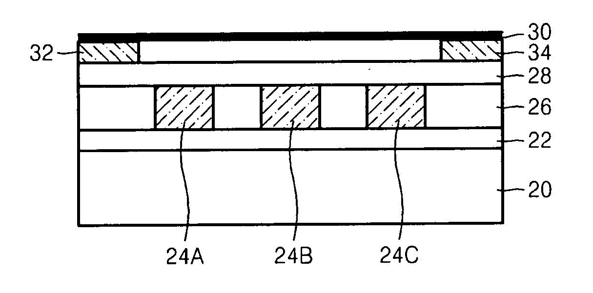
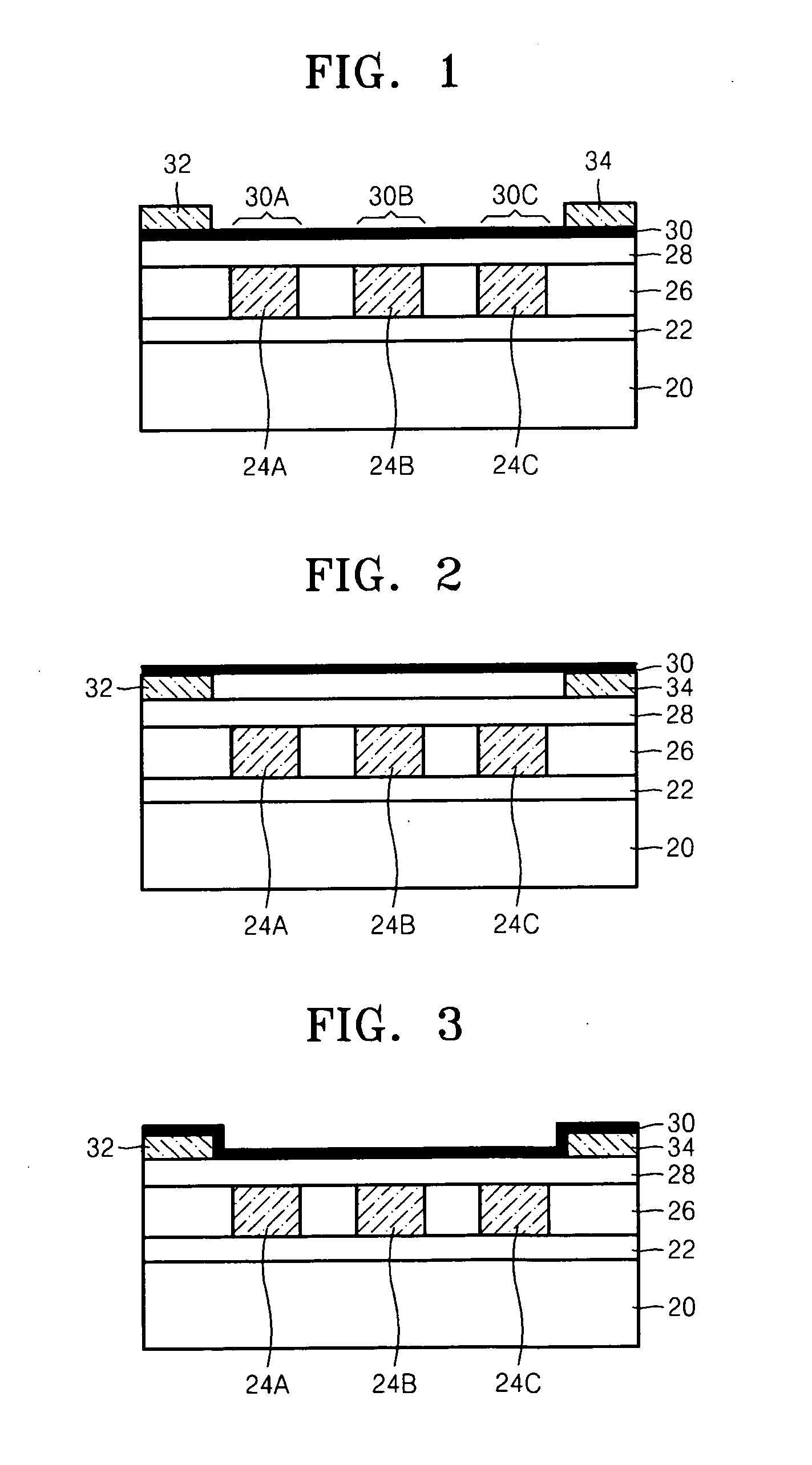
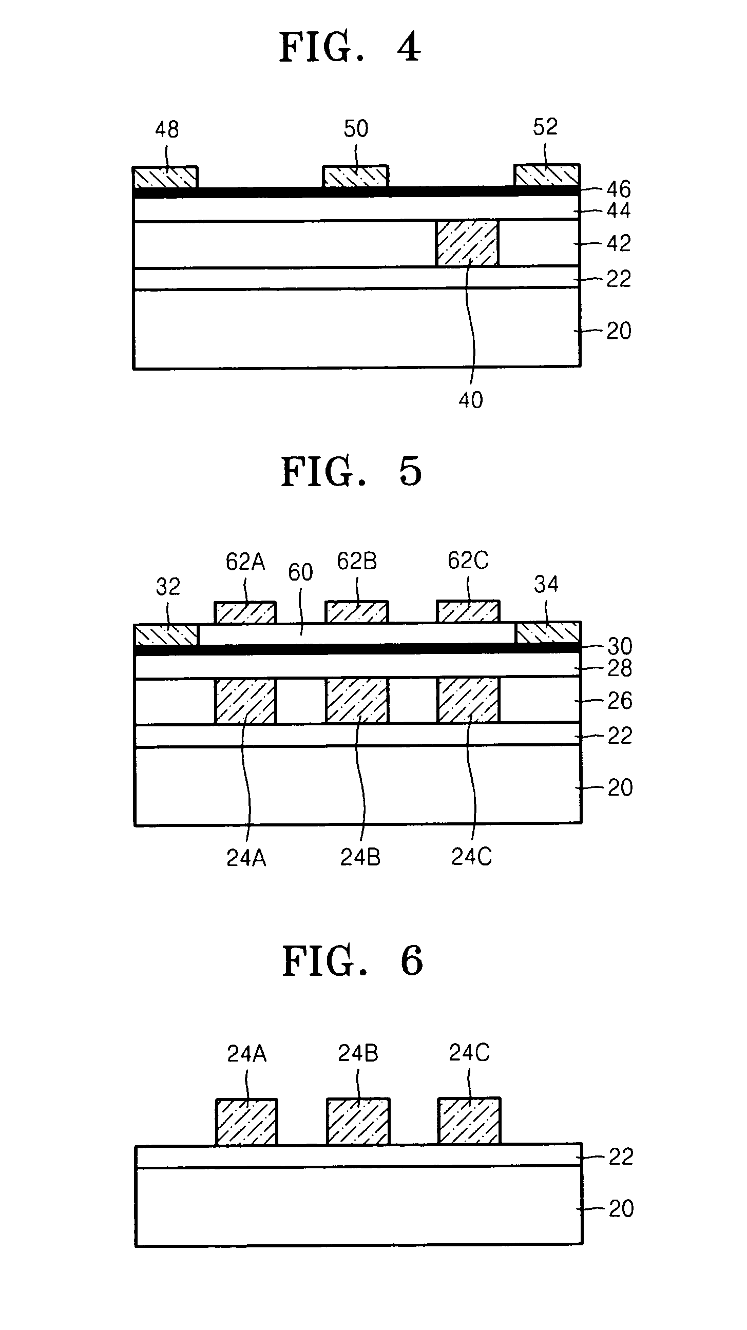
[0019]Hereinafter, a graphene device and a method of manufacturing the same according to example embodiments will be described in detail by explanation with reference to the attached drawings. In the drawings, the thicknesses of layers and regions are exaggerated for clarity. Example embodiments may, however, be embodied in many different forms and should not be construed as being limited to example embodiments set forth herein; rather, these example embodiments are provided so that this disclosure will be thorough and complete, and will fully convey the concept of example embodiments to those of ordinary skill in the art.

[0020]It will be understood that when an element is referred to as being “connected” or “coupled” to another element, it can be directly connected or coupled to the other element or intervening elements may be present. In contrast, when an element is referred to as being “directly connected” or “directly coupled” to another element, there are no intervening element...


PUM

PropertyMeasurementUnit
sizeaaaaaaaaaa
thicknessaaaaaaaaaa
thicknessaaaaaaaaaa

Abstract

Provided is a graphene device and a method of manufacturing the same. The graphene device may include an upper oxide layer on at least one embedded gate, and a graphene channel and a plurality of electrodes on the upper oxide layer. The at least one embedded gate may be formed on the substrate. The graphene channel may be formed on the plurality of electrodes, or the plurality of electrodes may be formed on the graphene channel.

Description

CROSS-REFERENCE TO RELATED APPLICATIONS[0001]This application claims priority under U.S.C. §119 to Korean Patent Application No. 10-2009-0098778, filed on Oct. 16, 2009, in the Korean Intellectual Property Office (KIPO), the entire contents of which are incorporated herein by reference.BACKGROUND[0002]1. Field[0003]Example embodiments relate to a graphene device and a method of manufacturing the same.[0004]2. Description of the Related Art[0005]Recently, research on graphene that can be used instead of semiconductor devices has been widely conducted. Graphene is a zero gap semiconductor. When a graphene nano-ribbon (GNR) is formed to have a channel width less than about 10 nm, a band gap may be formed due to a size effect. Accordingly, a field effect transistor capable of operating at room temperature may be manufactured by using the GNR.[0006]After the GNR is formed, an oxide layer having a thickness of about 300 nm may be formed thereon, and a global back gate may be formed on the...

Claims


Application Information

Patent Timeline
Patent Type & Authority Applications(United States)
IPC IPC(8): H03K3/01H01L29/775H01L21/335
CPCH01L29/1606H01L29/42384H01L29/78684H01L29/7781H01L29/78645H01L29/66742H01L21/2255
Inventor HEO, JIN SEONGSEO, SUN-AEKIM, DONG-CHULWOO, YUN-SUNGCHUNG, HYUN-JONG
Owner SAMSUNG ELECTRONICS CO LTD
Features
  • Generate Ideas
  • Intellectual Property
  • Life Sciences
  • Materials
  • Tech Scout
  • Unparalleled Data Quality
  • Higher Quality Content
  • 60% Fewer Hallucinations
Learn More