Array substrate for liquid crystal display device, liquid crystal display device and method of fabricating the same

Active Publication Date: 2011-04-28
LG DISPLAY CO LTD
View PDF1 Cites 42 Cited by
  • Summary
  • Abstract
  • Description
  • Claims
  • Application Information

AI Technical Summary

Benefits of technology

[0018]Accordingly, the present invention is directed to an array substrate, an LCD device and a method of fabrication t

Problems solved by technology

A signal delay is generated by the resistance deviation

Method used


Image

  • Array substrate for liquid crystal display device, liquid crystal display device and method of fabricating the same
  • Array substrate for liquid crystal display device, liquid crystal display device and method of fabricating the same
  • Array substrate for liquid crystal display device, liquid crystal display device and method of fabricating the same

Examples


first embodiment

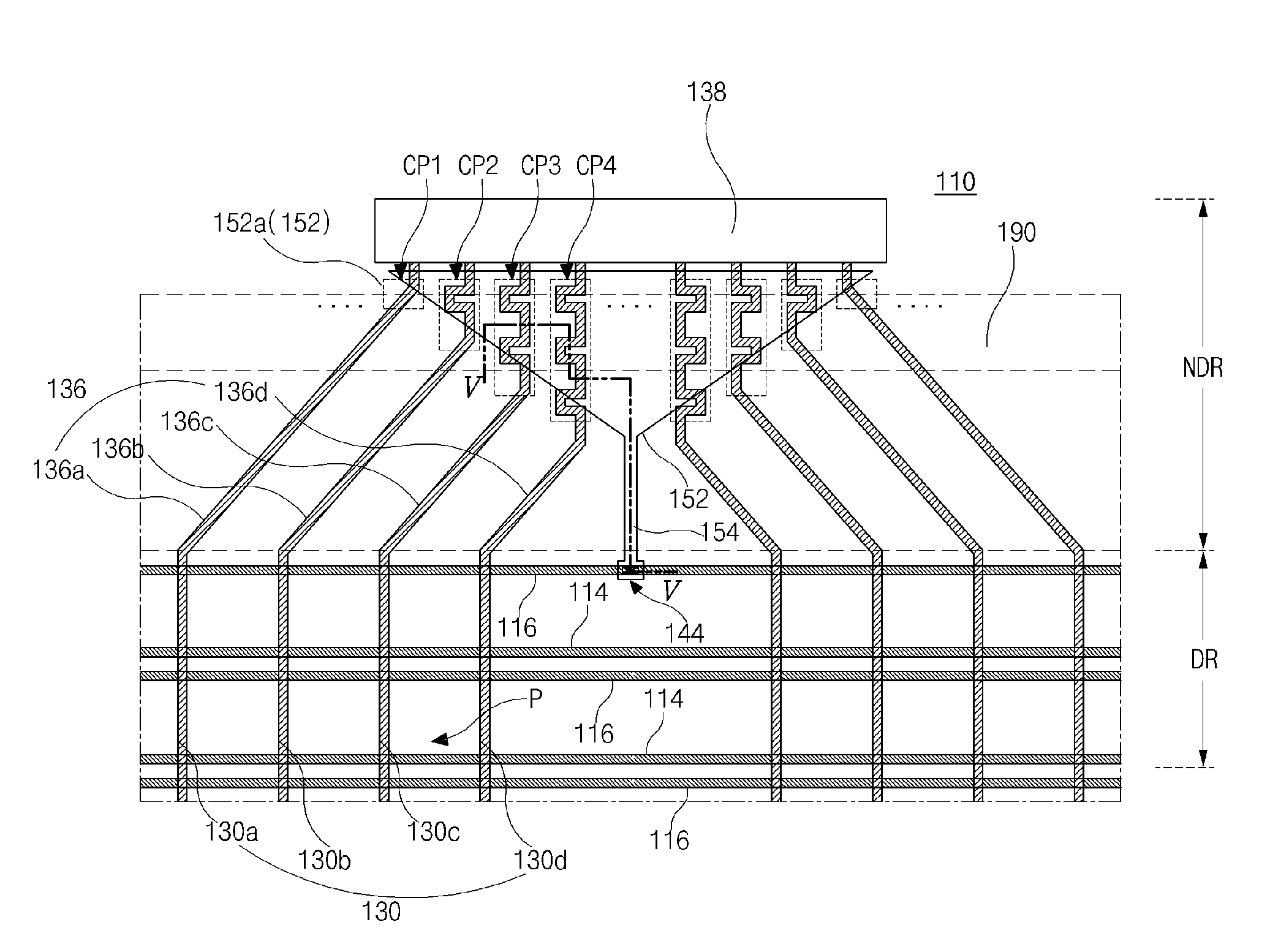
[0041]FIG. 3A is a plane view of an array substrate for an LCD device according to the present invention, and FIG. 3B is an enlarged plane view of one pixel region in FIG. 3A.

[0042]In FIGS. 3A and 3B, the array substrate 100 for the LCD device includes a substrate 110 where a display region DR and a non-display region NDR at a periphery of the display region DR are defined.

[0043]A plurality of gate lines 114 along a first direction and a plurality of data lines 130 are disposed on the substrate 110. The gate lines 114 and the data lines 130 cross each other to define a plurality of pixel regions P in the display region DR.

[0044]A plurality of common lines 116, which extends along the first direction, are disposed on the substrate 110. The common line 116 is parallel to and spaced apart from the gate line 114 and positioned between adjacent two gate lines 114. The common lines 116 also cross the data lines 130.

[0045]A plurality of data link lines 136 respectively extending from the d...

second embodiment

[0077]FIG. 6A is a plane view of an array substrate for an LCD device according to the present invention, and FIG. 6B is an enlarged plane view of one pixel region in FIG. 6A.

[0078]In FIG. 6A and 6B, the array substrate 200 for the LCD device includes a first substrate 210 where a display region DR and a non-display region NDR at a periphery of the display region DR are defined.

[0079]A plurality of gate lines 214 along a first direction and a plurality of data lines 230 are disposed on the first substrate 210. The gate lines 214 and the data lines 230 cross each other to define a plurality of pixel regions P in the display region DR.

[0080]A common line 216 is disposed on the first substrate 210 and in the non-display region NDR. Although not shown, the common line 216 applies a common voltage to a common electrode having a plate shape and disposed on a second substrate facing the first substrate 210.

[0081]A plurality of data link lines 236 respectively extending from the data lines ...

third embodiment

[0105]FIG. 9 is a cross-sectional view of an LCD device according to the present invention. In FIG. 9, the LCD device 300 includes a first substrate 310, a second substrate 360 facing the first substrate 310, a liquid crystal layer 380 interposed therebetween, and a seal pattern 390 for preventing leakage of the liquid crystal layer 380 at edges of the first and second substrates 310 and 360.

[0106]A display region DR and a non-display region NDR at a periphery of the display region DR are defined in the first substrate 310.

[0107]A plurality of gate lines (not shown) along a first direction and a plurality of data lines 330 are disposed on the substrate 310. The gate lines and the data lines 330 cross each other to define a plurality of pixel regions P in the display region DR.

[0108]A gate electrode 312 is disposed on the first substrate 310 and in the pixel region P, and a gate insulating layer 318 is disposed on the gate electrode 312. A semiconductor layer 320 including an active ...


PUM


Abstract

An array substrate for a liquid crystal display device includes a gate line on a substrate including a display region and a non-display region at a periphery of the display region; a common line on the substrate; a data drive integrated circuit in the non-display region; first and second data lines crossing the gate line to define a pixel region in the display region, the first and second data lines having a difference in a distance from the data drive integrated circuit; first and second data link lines connected to the data drive integrated circuit, the first and second data link lines respectively connected to the first and second data lines; a thin film transistor in the pixel region connected to the gate line and one of the first and second data lines; a pixel electrode in the pixel region and connected to the thin film transistor; and a first conductive pattern in the non-display region and connected to the common line such that a common voltage is applied to the first conductive pattern, the first conductive pattern overlapping the first and second data link lines to form first and second capacitors, respectively.

Description

[0001]The present application claims the benefit of Korean Patent Application Nos. 2009-0102511 and 2009-0103528, filed in Korea on Oct. 27, 2009 and Oct. 29, 2009, respectively, both of which are herein incorporated by reference.BACKGROUND OF THE INVENTION[0002]1. Field of the Invention[0003]The present invention relates to a liquid crystal display (LCD) device and more particularly to an array substrate for an LCD device and an LCD device being capable of uniformizing a signal delay in link lines, and a method of fabrication the array substrate and the LCD device.[0004]2. Discussion of the Related Art[0005]A related art liquid crystal display (LCD) device uses optical anisotropy and polarization properties of liquid crystal molecules. The liquid crystal molecules have a definite alignment direction as a result of their thin and long shapes. The alignment direction of the liquid crystal molecules can be controlled by applying an electric field across the liquid crystal molecules. I...

Claims


Application Information

Patent Timeline
IPC IPC(8): G02F1/1343H01L21/28
CPCG02F1/1333H01L27/124H01L27/1255G02F1/1368G02F1/1345
Inventor SHIM, SEOK HOSEOK, DAE YOUNG
Owner LG DISPLAY CO LTD
Why Eureka
Try Eureka