Light emitting device and electronic device

Inactive Publication Date: 2011-04-28
ELEMENT CAPITAL COMMERCIAL CO PTE LTD
View PDF2 Cites 8 Cited by
  • Summary
  • Abstract
  • Description
  • Claims
  • Application Information

AI Technical Summary

Benefits of technology

[0007]An advantage of some aspects of the invention is to provide a light emitting device and an electronic device that can solve at least one part of the above-described problems.
[0009]According to the first aspect of the invention, with respect to the light emitting element that emits a red light, an optical resonator in terms of satisfying Equation (ii) described later is not constituted. However, Equation (i) above is in agreement with the case where m in Equation (ii) is 0. With respect to the light emitting element, a kind of resonance conditions is established in such a meaning. Thus, according to the aspect of the invention, so-called perfect resonance conditions are not established but a certain light extraction efficiency improvement effect or a certain color purity improvement effect can be obtained. In addition, according to the aspect of the invention, with respect to the light emitting element that emits a red light, the fact that the resonance conditions are not satisfied does not change, and thus the viewing angle characteristics are improved.
[0012]According to this aspect, a resonance phenomenon can be preferably produced in the resonator structure containing a light emitting element, a reflective layer, and a translucent half-reflective layer. As described above, with respect to the light emitting element that emits a green light or a blue light, advantages in employing the resonator structure is larger than disadvantages in employing the resonator structure. Thus, producing differences in handling between the green and blue light emitting elements and the red light emitting elements brings preferable effects from the viewpoint of the whole light emitting device as in this aspect.
[0018]According to the aspect, since the electron-transporting layer and the second electrode layer are formed in common in all of the light emitting elements, the ease of manufacturing increases compared with the case where the respective layers are individually formed for every light emitting element. In the aspect of the invention, in spite of the fact that the light emitting element that emits a red light is constituted so that resonance conditions are not satisfied, the effect of the aspect can be obtained.
[0020]According to this aspect, the translucent half-reflective layer contains all or a part of the second electrode layer, in other words, the translucent half-reflective layer and all or a part of the second electrode layer is used in common or used for a dual purpose, and thus an increase in efficiency and simplification of the device structure is achieved and ease of manufacturing increases.
[0028]Since the electronic device of the aspect of the invention has the light emitting devices described above, an electronic device that can enjoy the improvement effect of the viewing angle characteristics in the light emitting element that emits a red light is provided.

Problems solved by technology

However, the techniques described in Japanese Patent Nos. 2797883 and 3555759 or techniques for strengthening light having a specific wavelength by an optical resonator have the following problems.
More specifically, according to the technique of Japanese Patent Nos. 2797883 and 3555759, a light having a specific wavelength can be surely strengthened by the action of a “micro optical resonator” (, , and the like of Japanese Patent No. 2797883) but the technique has a problem in that the degrees of advantages and disadvantages obtained by strengthening the light vary depending on the color to be strengthened.
However, the same does not always apply to the red light.
More specifically, although the light extraction efficiency improvement effect or the color purity improvement effect can be expected to some extent, the deterioration of the viewing angle characteristics exceeding the improvement is noticeable.

Method used


Image

  • Light emitting device and electronic device
  • Light emitting device and electronic device
  • Light emitting device and electronic device

Examples


Embodiment Construction

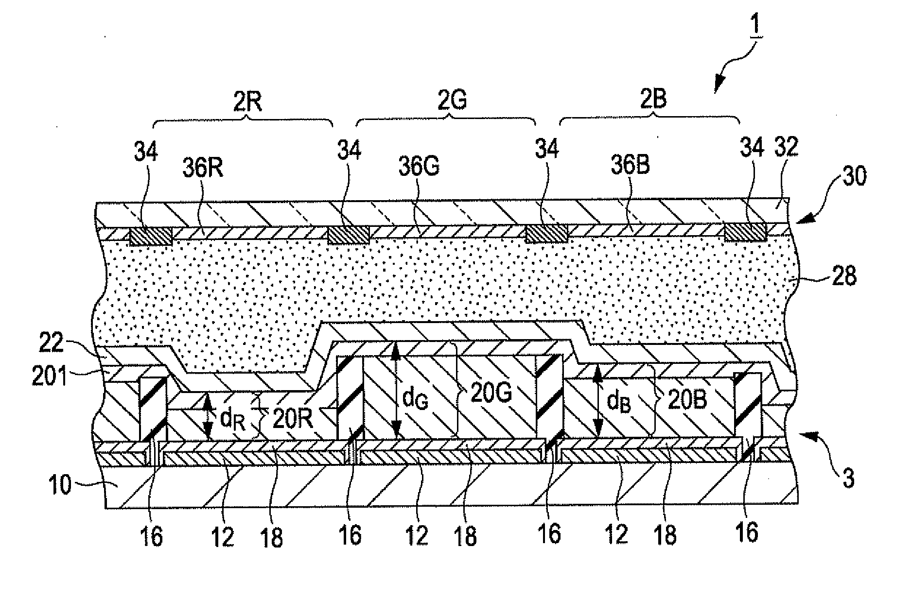
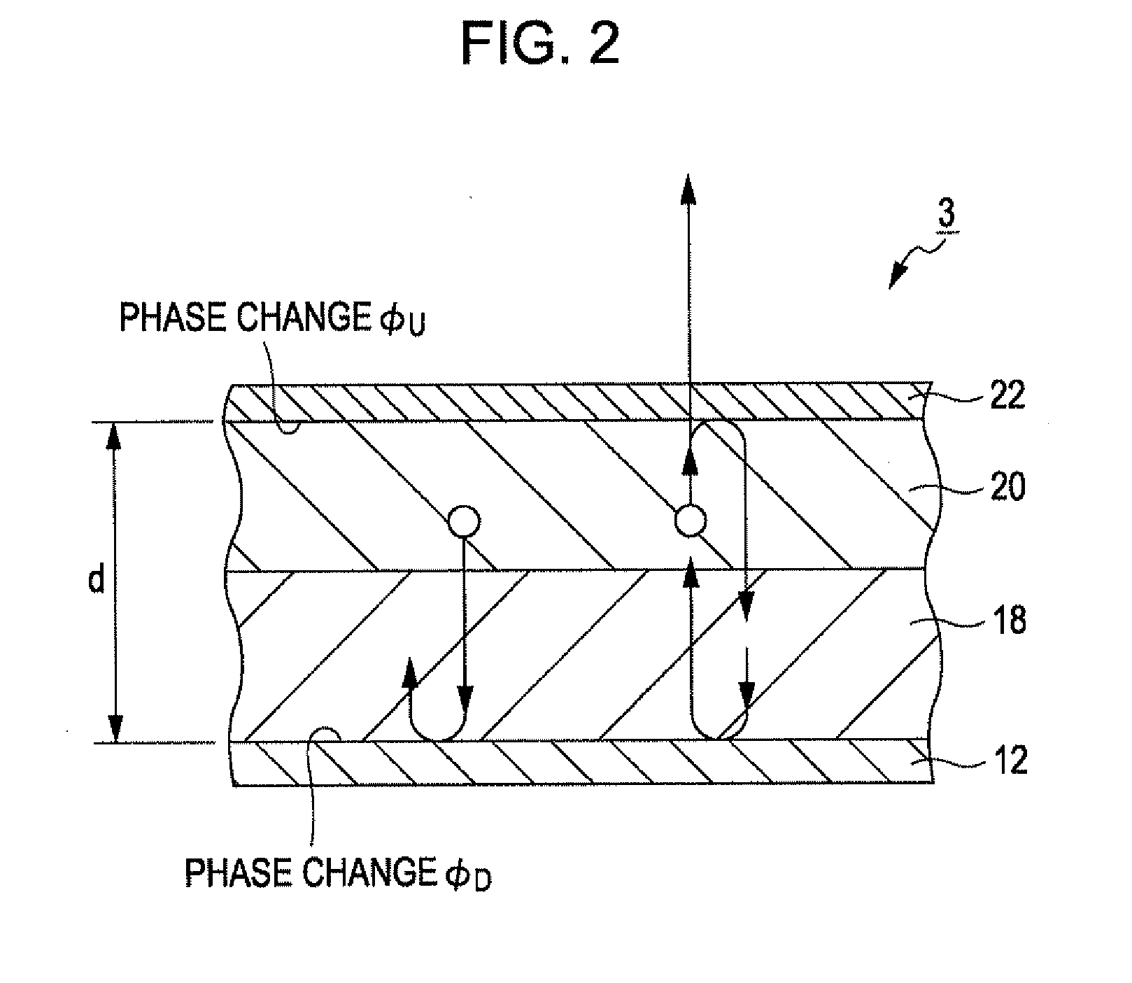
[0037]Hereinafter, embodiments of the invention will be described with reference to FIGS. 1 and 2. In addition to FIGS. 1 and 2 mentioned here, the ratio of the dimension of each part is sometimes made different from the actual dimension as appropriate in each drawing referred to below. Cross-sectional structure of organic EL device

[0038]FIG. 1 is a cross sectional view showing the outline of an organic EL device (light emitting device) 1 according to an embodiment of the invention. The organic EL device 1 has a light emitting panel 3 and a color filter panel 30.

[0039]The light emitting panel 3 has two or more light emitting elements (pixels) 2 (2R, 2G, 2B) as shown in FIG. 1. The organic EL device 1 of this embodiment is used as a full color image display device. The light emitting element 2R is a light emitting element in which the color of emitted light is red and the light emitting elements 2G and 2B are light emitting elements in which the color of emitted light is green or blu...


PUM


Abstract

A light emitting device has a plurality of light emitting elements each having a first electrode layer, a second electrode layer, and a light emitting layer disposed between the first and the second electrode layers, a reflective layer being disposed between a substrate and the first electrode layer and reflecting light emitted by the light emitting layer to the light emitting layer, the light emitting elements including a red light emitting element that emits a red light, a green light emitting element that emits a green light, and a blue light emitting element that emits a blue light, the green and the blue light emitting elements each having a resonator structure which contains the reflective layer and a translucent half-reflective layer and which is constituted by adjustment of the optical distance between the reflective layer and the translucent half-reflective layer, the red light emitting element not having the resonator structure.

Description

TECHNICAL FIELD[0001]The present invention relates to a light emitting device and an electronic device containing organic EL (electro luminescent) elements and the like.RELATED ART[0002]As thin and lightweight light emitting sources, OLED (organic light emitting diode), i.e., an organic EL (electro luminescent) element, has drawn attention, and image display devices having a large number of EL elements have been developed. The organic EL elements have a structure such that at least one layer of organic thin film formed with organic materials is sandwiched between a pixel electrode and a counter electrode.[0003]In the field of the organic EL elements, a technique for strengthening a light having a specific wavelength among emitted lights utilizing amplification interference, i.e., resonance, is known. In order to produce a resonance phenomenon, a reflective layer and a translucent half-reflective layer (“translucent” for taking out light) are utilized. This technique can increase the...

Claims


Application Information

Patent Timeline
IPC IPC(8): F21V9/00
CPCH01L51/5265H01L27/322H10K59/38H10K59/876H10K50/852
Inventor ODA, TOSHIHIRO
Owner ELEMENT CAPITAL COMMERCIAL CO PTE LTD
Why Eureka
Try Eureka