Organic Light Emitting Display Apparatus and Method of Manufacturing the Same

a technology of light-emitting display and organic light-emitting apparatus, which is applied in the direction of electrical apparatus, basic electric elements, semiconductor devices, etc., can solve the problems of increasing the frequency of photolithography method using masks, increasing the manufacturing time complicated manufacturing process so as to improve the electric characteristics of organic light-emitting display apparatus and simplify the manufacturing process

Active Publication Date: 2011-05-19
SAMSUNG DISPLAY CO LTD
View PDF8 Cites 31 Cited by
  • Summary
  • Abstract
  • Description
  • Claims
  • Application Information

AI Technical Summary

Benefits of technology

Aspects of embodiments of the present invention are directed toward an organic light emitting display apparatus and a method of manufacturing the organic light emitting apparatus, wherein the manufacturing process of the organic light emitting display apparatus may be simplified and the electric characteristics of the organic light emitting display apparatus may be improved.

Problems solved by technology

Thus, the frequency that the photolithography method using a mask is used is increased, the manufacturing process of the organic light emitting display apparatus is complicated, and the manufacturing time thereof is increased.
Also, it is difficult to control the manufacturing process and thus many defects may occur.

Method used


Image

  • Organic Light Emitting Display Apparatus and Method of Manufacturing the Same
  • Organic Light Emitting Display Apparatus and Method of Manufacturing the Same
  • Organic Light Emitting Display Apparatus and Method of Manufacturing the Same

Examples


Embodiment Construction

Reference will now be made in detail to embodiments, examples of which are illustrated in the accompanying drawings, wherein like reference numerals refer to the like elements throughout. In this regard, the present embodiments may have different forms and should not be construed as being limited to the descriptions set forth herein. Accordingly, the embodiments are merely described below, by referring to the figures, to explain aspects of the present description.

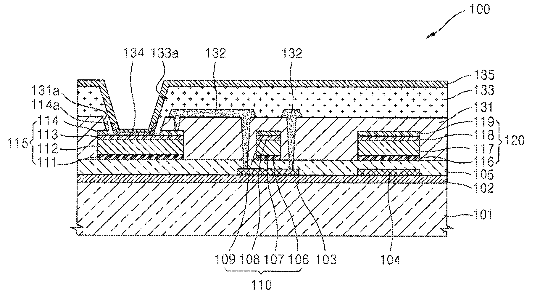
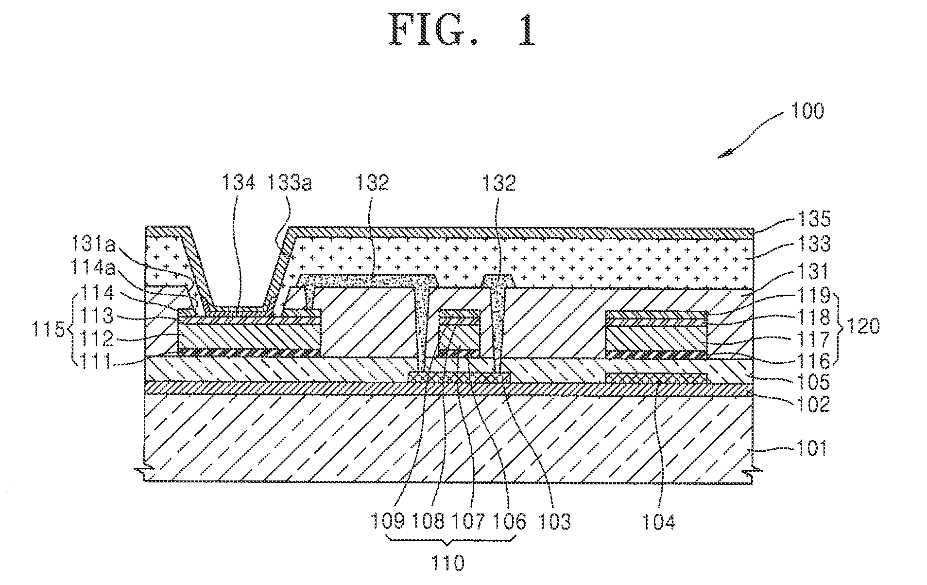
FIG. 1 is a cross-sectional view of an organic light emitting display apparatus 100 according to an embodiment of the present invention.

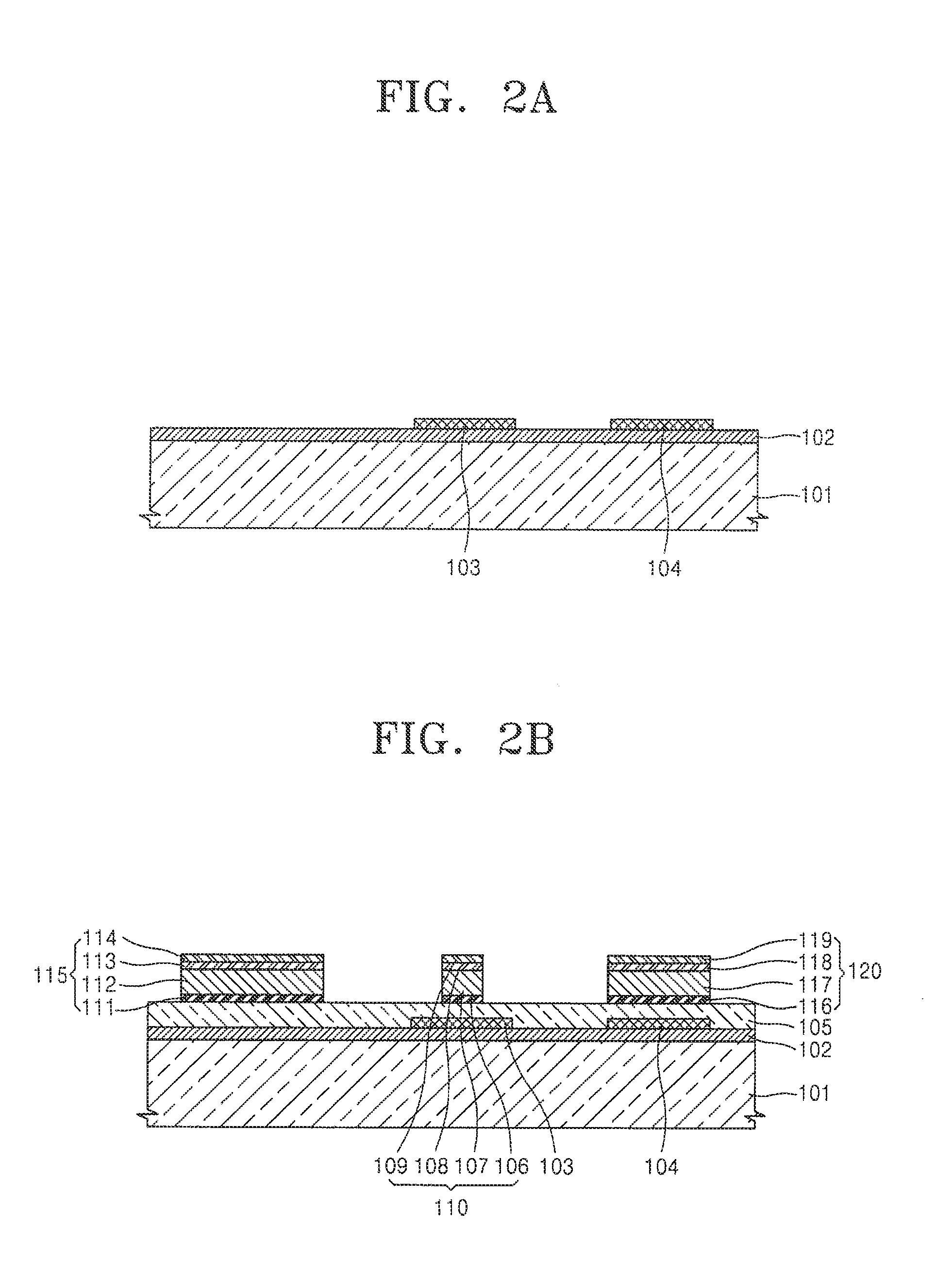
The organic light emitting display apparatus 100 includes a substrate 101, an active layer 103, a gate electrode 110, a pixel electrode 115, a source / drain electrode 132, an intermediate layer 134, and a counter electrode 135.

The substrate 101 may be formed of transparent glass containing SiO2 as a main component, but is not limited thereto. For example, the substrate 101 may also be formed...


PUM


Abstract

An organic light emitting display apparatus and a method of manufacturing the organic light emitting display apparatus, whereby the manufacturing process is simplified and the electric characteristics of the organic light emitting display apparatus are improved. The organic light emitting display apparatus includes: a gate electrode that includes a first conductive layer including ITO, a second conductive layer on the first conductive layer, a third conductive layer on the second conductive layer and including ITO, and a fourth conductive layer on the third conductive layer and including IZO or AZO; and a pixel electrode formed in the same layer level as the gate electrode and including a first electrode layer that includes ITO, a second electrode layer on the first electrode layer, a third electrode layer on the second electrode layer and including ITO, and a fourth electrode layer on the third electrode layer and including IZO or AZO.

Description

CROSS-REFERENCE TO RELATED APPLICATIONThis application claims priority to and the benefit of Korean Patent Application No. 10-2009-0109706, filed on Nov. 13, 2009, in the Korean Intellectual Property Office, the entire content of which is incorporated herein by reference.BACKGROUND1. FieldOne or more embodiments of the present invention relate to an organic light emitting display apparatus and a method of manufacturing the same, and more particularly, to an organic light emitting display apparatus and a method of manufacturing the same, in which manufacturing processes may be simplified and electric characteristics of the organic light emitting display apparatus may be improved.2. Description of the Related ArtDevelopments in display technology have led to the replacement of conventional display apparatus with portable, thin flat panel display apparatuses. From among the flat panel apparatuses, an electroluminescent display apparatus, which is a self-emissive display apparatus, has ...

Claims


Application Information

Patent Timeline
Patent Type & Authority Applications(United States)
IPC IPC(8): H01L51/52H01L51/56
CPCH01L51/5215H01L27/3248H10K59/123H10K50/816H01L29/4958
Inventor PARK, SUNYOU, CHUN-GIPARK, JONG-HYUNKANG, JIN-HEELEE, YUL-KYU
Owner SAMSUNG DISPLAY CO LTD
Why Eureka
Try Eureka