Surface acoustic wave element

a surface acoustic wave element and acoustic wave element technology, applied in piezoelectric/electrostrictive/magnetostrictive devices, piezoelectric/electrostriction/magnetostriction machines, electrical equipment, etc., can solve the problems of low insufficient electrical power handling capability of surface acoustic wave elements for high-frequency applications and high-power applications, etc., to dramatically increas

Inactive Publication Date: 2011-05-19
MURATA MFG CO LTD
View PDF3 Cites 23 Cited by
  • Summary
  • Abstract
  • Description
  • Claims
  • Application Information

AI Technical Summary

Benefits of technology

[0013]It is believed that when the Al electrode layer has an average crystal grain size of about 60 nm or less, most of the grain boundaries have twin crystal structures with atomic level widths. Accordingly, the activation energy of the Al electrode layer is close to the activation energy in a bulk state, such that the electrical power handling capability can be dramatically increased. Therefore, preferred embodiments of the present invention provide a surface acoustic wave element having a high electrical power handling capability.

Problems solved by technology

Unfortunately, Al has a low electrical power handling capability.
The hillock or the void may cause short-circuiting of the electrode and result in destruction of the surface acoustic wave element.
However, the electrical power handling capability of the surface acoustic wave elements described above are insufficient for use in high-frequency applications and high-power applications.

Method used


Image

  • Surface acoustic wave element
  • Surface acoustic wave element
  • Surface acoustic wave element

Examples


Embodiment Construction

[0019]An exemplary preferred embodiment of the invention will now be described.

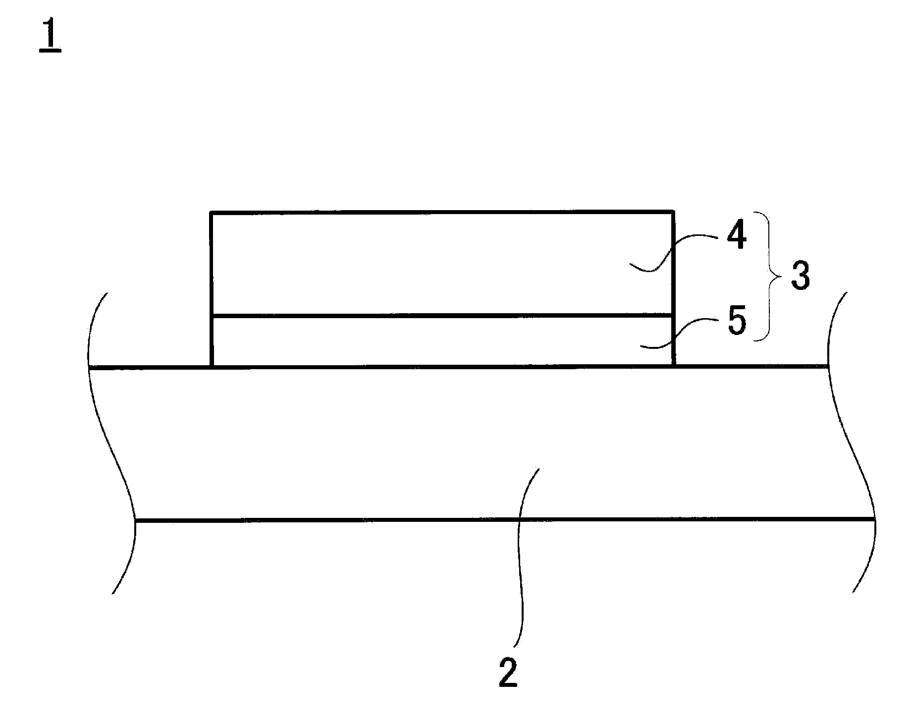
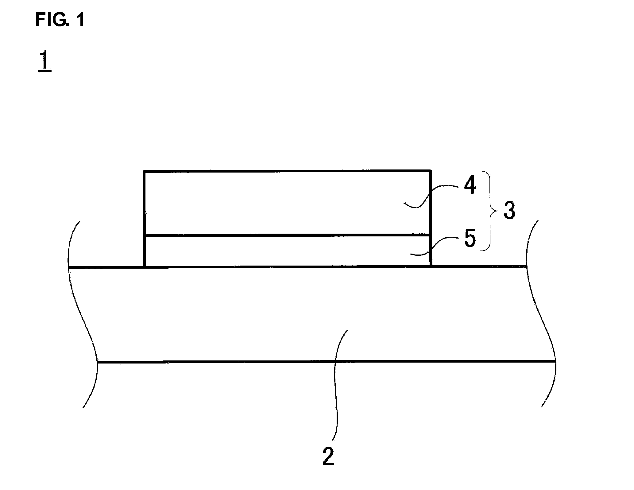
[0020]FIG. 1 is a fragmentary sectional view showing main portions of a surface acoustic wave element 1 according to a preferred embodiment of the present invention. FIG. 1 shows a portion in which an electrode 3 is disposed on a piezoelectric substrate 2.

[0021]The piezoelectric substrate 2 is preferably made of a LiTaO3 or LiNbO3 single crystal, for example. The electrode 3 includes an Al electrode layer 4 and a base electrode layer 5.

[0022]The base electrode layer 5 is disposed on the piezoelectric substrate 2. The base electrode layer 5 is provided to improve the adhesion between the piezoelectric substrate 2 and the Al electrode layer 4. The base electrode layer 5 preferably primarily includes at least either Ti or Cr, for example. The Al electrode layer 4 is disposed on the base electrode layer 5. The Al electrode layer 4 preferably includes, for example, Al or an Al-based alloy as the main component...


PUM


Abstract

A surface acoustic wave element includes a piezoelectric substrate made of a LiNbO3 or LiTaO3 single crystal, a base electrode layer disposed on the piezoelectric substrate and primarily including at least one of Ti and Cr, and an Al electrode layer primarily including Al disposed on the base electrode layer. The Al electrode layer is an epitaxially grown film with an orientation, and has a twin crystal structure exhibiting six-fold symmetry spots in an XRD pole figure. The average grain size of the Al electrode layer is about 60 nm or less.

Description

BACKGROUND OF THE INVENTION[0001]1. Field of the Invention[0002]The present invention relates to surface acoustic wave elements, and particularly, to a surface acoustic wave element including an electrode layer primarily including Al and having a twin crystal structure.[0003]2. Description of the Related Art[0004]The surface acoustic wave element is an electronic component using surface acoustic waves that propagate mechanical vibration energy. The surface acoustic wave element typically includes a piezoelectric substrate, and an interdigital transducer (IDT electrode) on the piezoelectric substrate through which a signal is applied to or extracted from the surface acoustic wave element.[0005]The IDT electrode is typically made of a material having a low electrical resistivity and a low specific gravity, such as Al or an Al-based alloy. Unfortunately, Al has a low electrical power handling capability. If a high power is applied to the Al electrode, a hillock or a void may be produce...

Claims


Application Information

Patent Timeline
Patent Type & Authority Applications(United States)
IPC IPC(8): H01L41/047
CPCH03H3/08H03H9/14541H03H9/02929
Inventor KONISHI, YOSHIYUKIFUKUDA, SHINICHI
Owner MURATA MFG CO LTD
Why Eureka
Try Eureka