Organic Photoelectric Device

a photoelectric device and organic technology, applied in the field of organic photoelectric devices, can solve the problems of reducing the maximum usable device size, limiting the maximum light emitting surface area, and adhesive regions, etc., and achieves the effects of reducing the inactive edge region, reducing the resistance of sheets, and reducing the inactive edge area

Inactive Publication Date: 2011-05-26
FRAUNHOFER GESELLSCHAFT ZUR FOERDERUNG DER ANGEWANDTEN FORSCHUNG EV
View PDF3 Cites 44 Cited by
  • Summary
  • Abstract
  • Description
  • Claims
  • Application Information

AI Technical Summary

Benefits of technology

[0022]One advantage of the present invention is that, by using an electrically conductive cover member, or a cover member having an electrically conductive coating, reduction of the inactive edge regions of an organic photoelectric device is enabled, which therefore leads to a larger optically active area of the organic photoelectric device.
[0023]In particular, due to utilization of an electrically conductive cover member, or a cover member having an electrically conductive coating, in embodiments of the invention, the metal meshes described in conventional technology for reducing the sheet resistance may be dispensed with, as a result of which the optically active area of the organic photoelectric device is increased further, and / or the manufacturing expenditure is reduced, and / or the light emission capability increases.
[0024]In addition, the conductive coating of the self-supporting cover member, or the conductive self-supporting cover member, which are both easy to produce, enables input of the power into the electrically conductive coating or cover member at only one terminal, from the outside, on a housing of the organic photoelectric device, which results in further improvement of the area utilization ratio.
[0025]Embodiments of organic photoelectric devices may be configured, for example, as an OLED (organic light emitting diode), an OLED structure, or as an OPVC (organic photovoltaic cell / organic solar cell).
[0026]An organic light emitting diode will also be referred to as OLED for short in the following. An organic photovoltaic cell will also be referred to in the following as an organic solar cell, or as OPVC for short. An organic photoelectric device will also be referred to in the following as OLED / OPVC for short.
[0027]A self-supporting cover member will in the following sometimes also be referred to as an encapsulation element.

Problems solved by technology

Since OLEDs are current-operated devices, an important issue in the manufacture of large-area light emission elements is homogeneous current density distribution on large areas.
Due to the low conductivity of said TCOs, said layers limit the maximum light emitting surface area.
In this case, too, the transparent electrical contact reduces the maximally usable device size.
Said adhesive region, which cannot be minimized to any extent desired in order to ensure a barrier effect toward air and to ensure mechanical stability, is not available for the active light emitting area.
With large-area devices, the high resistance of the transparent layer (about 10-100 ohm / square), i.e. of the ITO layer, or top electrode, leads to inhomogeneity of the power input, since the contacts of the layer are possible only on the edge of the light emission element.
Due to their non-transparency, said grids, or webs, reduce the effective surface area of the device.
A useful improvement would be to increase the grid metal thickness, or the thickness of the lines of the metal mesh, which is not useful, however, due to the structuring possibilities and layer thicknesses of the organic layers.
A further problem are the cover glasses for encapsulating the OLED / OPVC elements, which may have cavities in order to receive the functional layers and absorption materials.
In addition, the production process has a high potential of damaging the environment due to the etching chemicals used.

Method used


Image

  • Organic Photoelectric Device
  • Organic Photoelectric Device
  • Organic Photoelectric Device

Examples


first embodiment

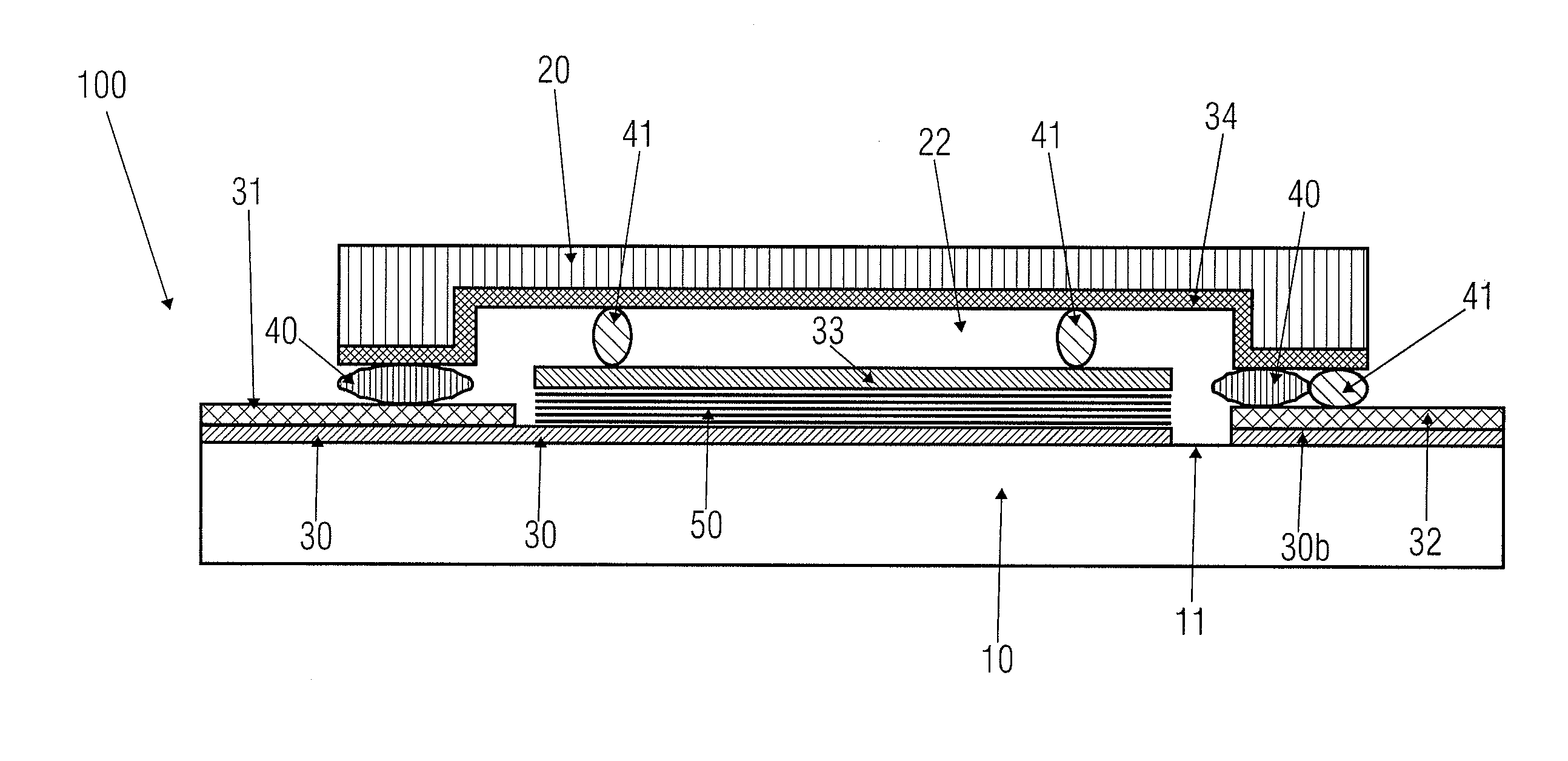
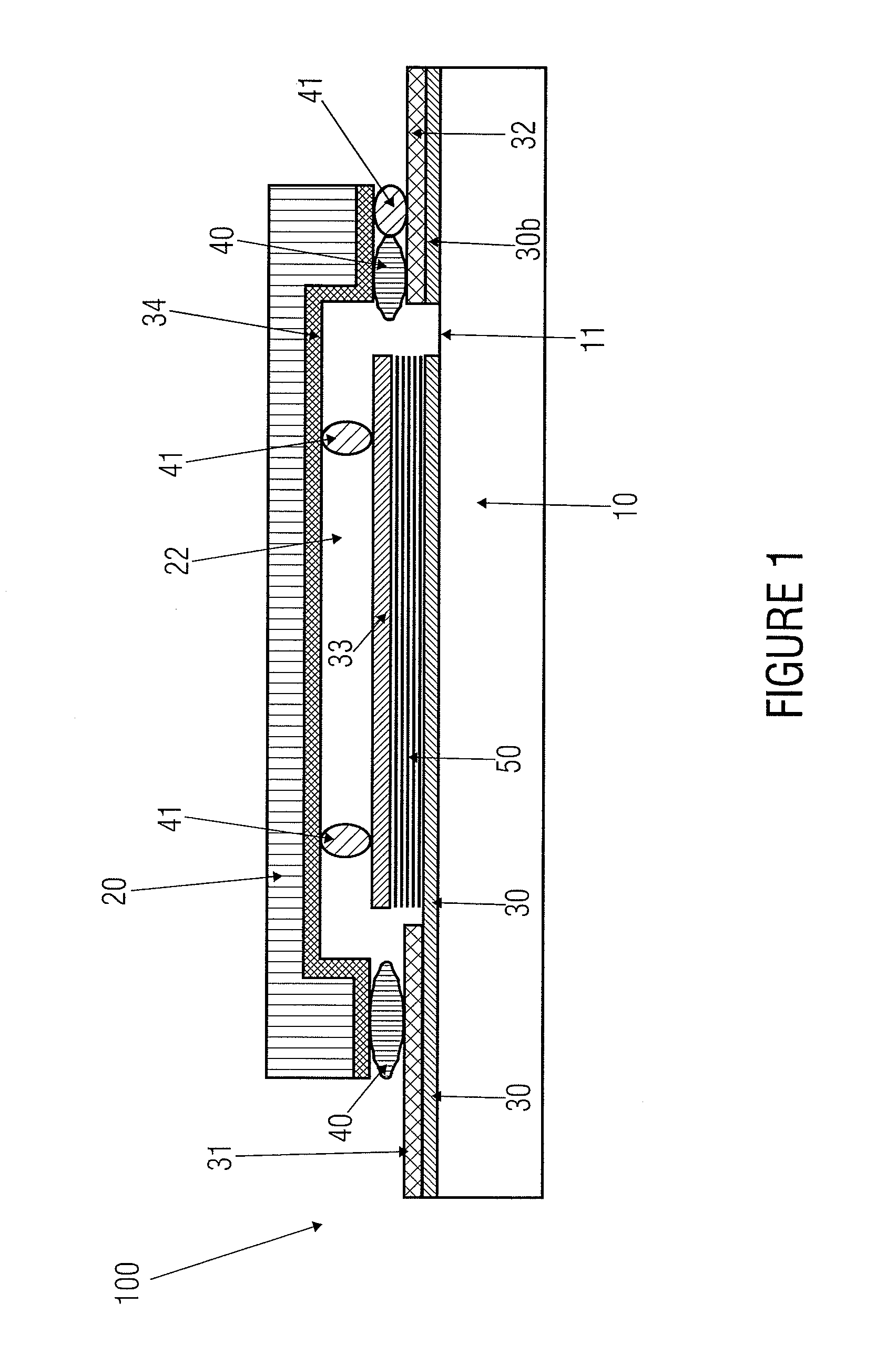
[0043]FIG. 1 shows a sectional view of an organic photoelectric device in accordance with the present invention. The organic photoelectric device 100 comprises a substrate 10, which includes a surface 11. The surface 11 has a base electrode 30a as well as an electrically insulated partial base electrode 30b formed thereon. Following this, a roof electrode 33 is formed, so that an organic functional layer 50 is arranged between the roof electrode 33 and the base electrode 30. The lateral extension of the organic functional layer 50 is the same, for example, as the lateral extension of the roof electrode, or deviates only slightly therefrom. The base electrode 30a has a substrate metallization 31 on one of its edges on a surface facing away from the surface 11. On a surface facing away from the surface 11, the partial base electrode 30b has a substrate metallization 32, which corresponds, for example, to the partial base electrode 30b in terms of lateral dimensions, or deviates only s...

second embodiment

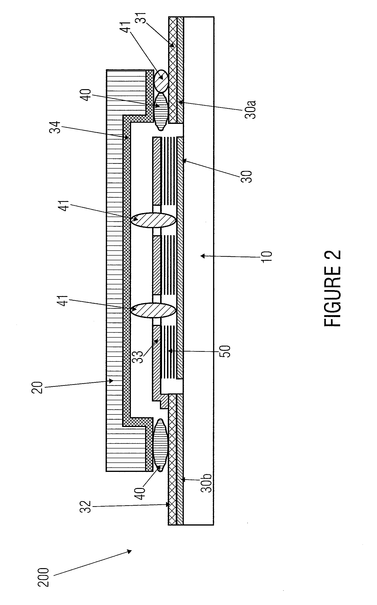
[0055]FIG. 2 shows a sectional view of an organic photoelectric device 200 in accordance with the present invention. The organic photoelectric device 200 comprises a substrate 10, which includes a surface 11. The surface 11 has a base electrode 30, a first partial base electrode 30a and a second partial base electrode 30b formed thereon. Following this, a roof electrode 33 is formed, so that an organic functional layer 50 is arranged between the roof electrode 33 and the base electrode 30. The lateral extension of the organic functional layer 50 is the same, for example, as the lateral extension of the roof electrode, or deviates only slightly therefrom. On a surface facing away from the surface 11, the first partial base electrode 30a has a substrate metallization 31, which corresponds, for example, to the first partial base electrode 30a in terms of lateral dimensions, or deviates only slightly from same. On a surface facing away from the surface 11, the second partial base electr...

third embodiment

[0059]FIG. 3 shows a sectional view of an organic photoelectric device 300 in accordance with the present invention. The organic photoelectric device 300 shown in FIG. 3 differs from the organic photoelectric device 100 shown in FIG. 1 in that, instead of a glass provided with cavities 22, a planar no-cavity glass substrate is used as the cover glass 20. Instead of producing the depressions or cavities in a subtractive manner by means of etching, an encapsulation edge is created on the edges of the cover glass 20 by means of a glass frit paste fused in a structured manner, which glass frit paste implements the distance—useful for the active layers and / or the organic functional layer 50 and for the accommodation of getter materials—between the coated substrate 100 and the cover glass substrate, or cover glass 20.


PUM


Abstract

An organic photoelectric device includes a substrate, a base electrode, an electrode terminal, a roof electrode, an organic functional layer, and a self-supporting cover member. The base electrode is configured above a first surface of the substrate, and the electrode terminal is accessible from above the first surface of the substrate. The self-supporting cover member serves to encapsulate the organic functional layer, which is arranged between the substrate and the self-supporting cover member, the self-supporting cover member being formed from conductive material or being coated with a conductive material on a side facing the substrate. The conductive material is locally coupled, in an electrically conductive manner, to the base electrode or the roof electrode at laterally distributed locations, and is further coupled to the electrode terminal in an electrically conductive manner.

Description

CROSS-REFERENCE TO RELATED APPLICATIONS[0001]This application claims priority from German Patent Application No. 102009046755.6, which was filed on Nov. 17, 2009, and is incorporated herein in its entirety by reference.[0002]The present invention relates to an organic photoelectric device such as an organic light emitting diode or an organic photocell, for example.BACKGROUND OF THE INVENTION[0003]On the basis of organic light emitting diodes (OLEDs), novel area light elements can be realized. As two-dimensional illuminants whose luminance is moderate as compared to that of LEDs, OLEDs are ideally suited for manufacturing two-dimensional diffuse light sources. Said light sources are predicted to see a tumultuous development similar to that of displays based on OLEDs. Due to their thin-layer technology, OLEDs may also enable, in the distant future, realizing flexible illuminants that allow entirely new applications in terms of illumination of spaces, or rooms.[0004]Since OLEDs are cur...

Claims


Application Information

Patent Timeline
Patent Type & Authority Applications(United States)
IPC IPC(8): H01L51/50
CPCH01L27/301H01L51/448H01L51/5237Y02B10/12H01L51/5243H01L2251/5361Y02E10/549H01L51/5203H01L51/525Y02B10/10Y02P70/50H10K39/10H10K30/88H10K50/805H10K50/8423H10K50/8428H10K50/8426
Inventor HESSE, JANAMELUNG, JOERGKIRCHHOF, CHRISTIAN
Owner FRAUNHOFER GESELLSCHAFT ZUR FOERDERUNG DER ANGEWANDTEN FORSCHUNG EV
Why Eureka
Try Eureka