Bidirectional power switch controllable to be turned on and off

Active Publication Date: 2011-05-26
STMICROELECTRONICS (TOURS) SAS +1
View PDF4 Cites 27 Cited by
  • Summary
  • Abstract
  • Description
  • Claims
  • Application Information

AI Technical Summary

Benefits of technology

[0014]An object of an embodiment of the present invention is to overcome at least some of the

Problems solved by technology

However, a vertical MOS transistor is unidirectional and it is necessary to associate it with a diode bridge if an A.C. current is desired to be conducted.
This association has the disadvantage of having a non-negligible voltage drop in the on state.
However, this component has the disadvantage of not being controllable to be turned off, unless a complex control circuit is associated thereto.
The symmetrical structure of FIG. 2, however, c

Method used


Image

  • Bidirectional power switch controllable to be turned on and off
  • Bidirectional power switch controllable to be turned on and off
  • Bidirectional power switch controllable to be turned on and off

Examples


Example

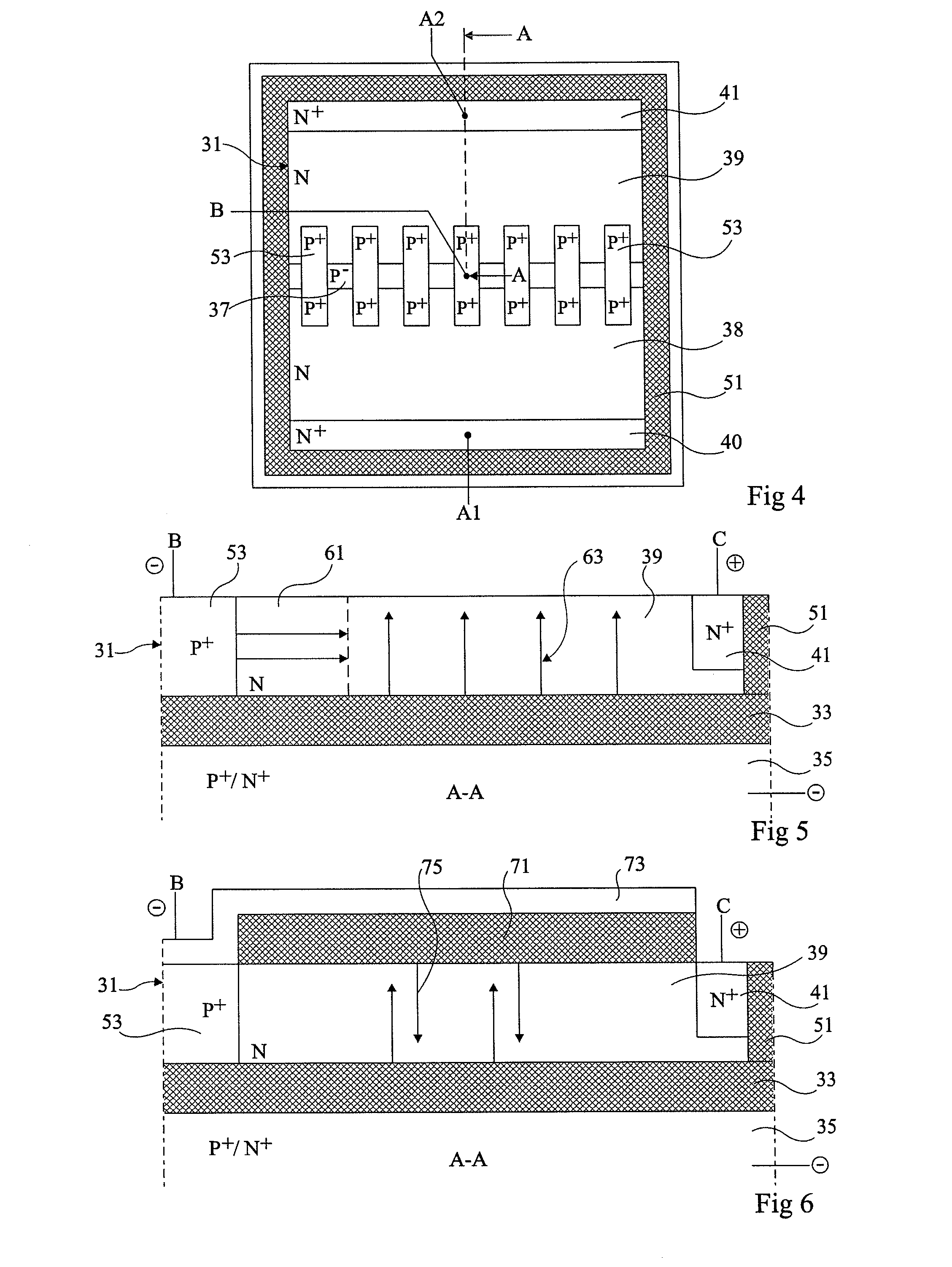
[0039]For clarity, the same elements have been designated with the same reference numerals in the different drawings and, further, as usual in the representation of integrated circuits, the various drawings are not to scale.

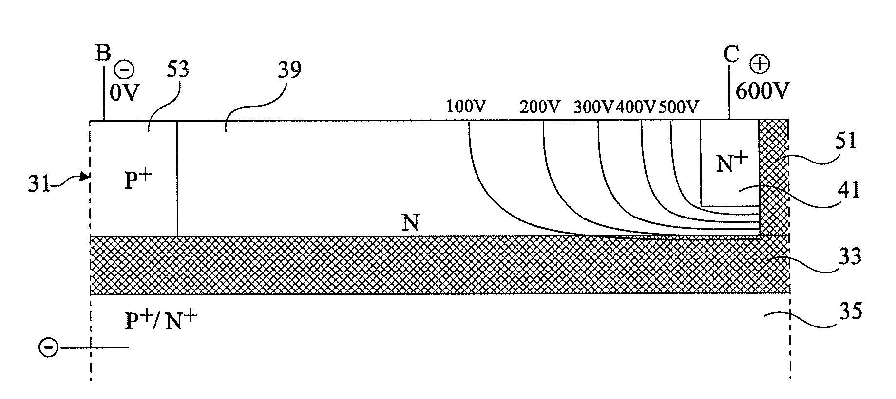
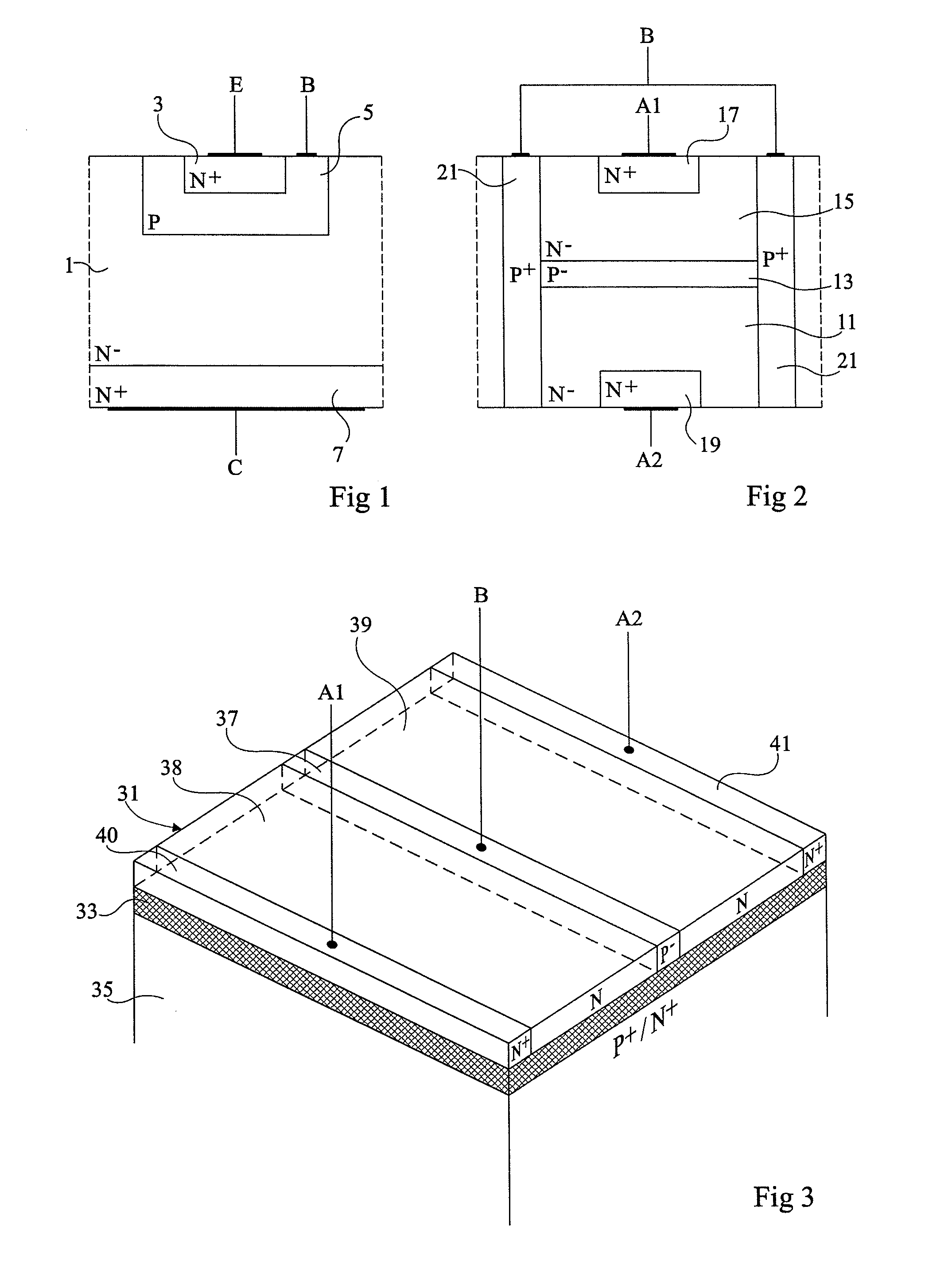
[0040]FIG. 3 is a perspective view of a bidirectional transistor according to an embodiment of the present invention. Unlike known power transistors, which are generally vertical, the transistor of FIG. 3 is horizontal. This enables to do away with the issues of the forming of deep thin bases of the vertical symmetrical transistors and of the problems caused by the presence of wells of access to these bases.

[0041]The transistor is formed in a semiconductor layer 31 which extends on an insulating layer 33, insulating layer 33 extending on a heavily-doped semiconductor wafer 35 biased to a reference voltage. In the shown example, the transistor is an NPN transistor. It should be noted that a PNP transistor can be manufactured in the same way, by inverting all condu...


PUM


Abstract

A bidirectional power transistor formed horizontally in a semiconductor layer disposed on a heavily-doped semiconductor wafer with an interposed insulating layer, the wafer being capable of being biased to a reference voltage, the product of the average dopant concentration and of the thickness of the semiconductor layer ranging between 5·1011 cm−2 and 5·1012 cm−2.

Description

CROSS REFERENCE TO RELATED APPLICATIONS[0001]This application claims the priority benefit of French patent application Ser. No. 09 / 58310, filed on Nov. 24, 2009, entitled “BIDIRECTIONAL POWER SWITCH CONTROLLABLE TO BE TURNED ON AND OFF,” which is hereby incorporated by reference to the maximum extent allowable by law.BACKGROUND OF THE INVENTION[0002]1. Field of the Invention[0003]The present invention relates to a monolithic bidirectional power switch controllable on and off.[0004]2. Discussion of the Related Art[0005]The term “power switch” is here used to designate a switch capable of switching at voltages greater than 100 volts and / or at currents greater than 1 ampere. A power switch is for example intended to switch the power supply of a load connected to the mains. A power switch is generally formed vertically in a semiconductor substrate, that is, the current between the main electrodes of the switch flows between the upper and lower surfaces of the semiconductor substrate. Th...

Claims


Application Information

Patent Timeline
IPC IPC(8): H01L29/78H01L29/73
CPCH01L29/063H01L29/08H01L29/735H01L29/402H01L29/36
Inventor QUOIRIN, JEAN-BAPTISTEPHUNG, LUONG VI TBATUT, NATHALIE
Owner STMICROELECTRONICS (TOURS) SAS
Why Eureka
Try Eureka