

Method for removal of residue from a magneto-resistive random access memory (MRAM) film stack using a sacrificial mask layer
- Summary
- Abstract
- Description
- Claims
- Application Information
AI Technical Summary
Benefits of technology
Problems solved by technology
Method used
Image

Examples
Embodiment Construction
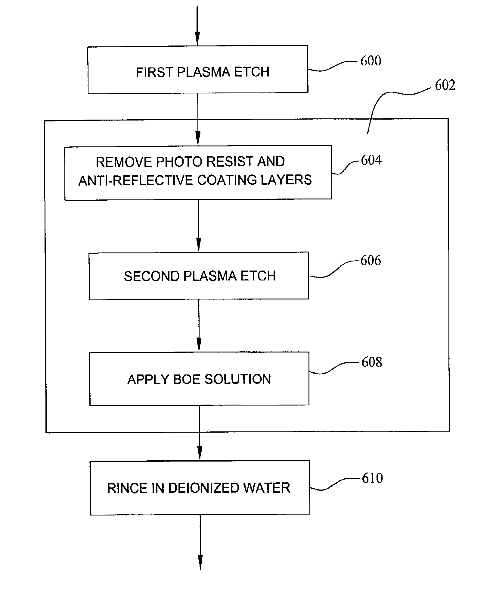
[0021]The present invention is a method for removal of residues produced by plasma etching a magneto resistive random access memory (MRAM) film stack. The film stack contains a photoresist layer, an anti-reflective coating layer, a sacrificial layer, a conductive layer, a layer or layers of magnetic material and a tunneling layer. The sacrificial top layer, such as for example SiO2, is used as a hard mask for etching a layer or layers of magnetic material to the tunneling layer, such as for example alumina. Following a chlorine-based or fluorine based chemistry etching of the sacrificial top layer and conductive layer, a photoresist strip and an oxygen and chlorine-mixed chemistry etching for high selectivity to the tunneling layer, the residues, including the presence of any “veil”-like structures, as well as the sacrificial top layer, are removed using a buffered oxide etch (BOE) wet dip.
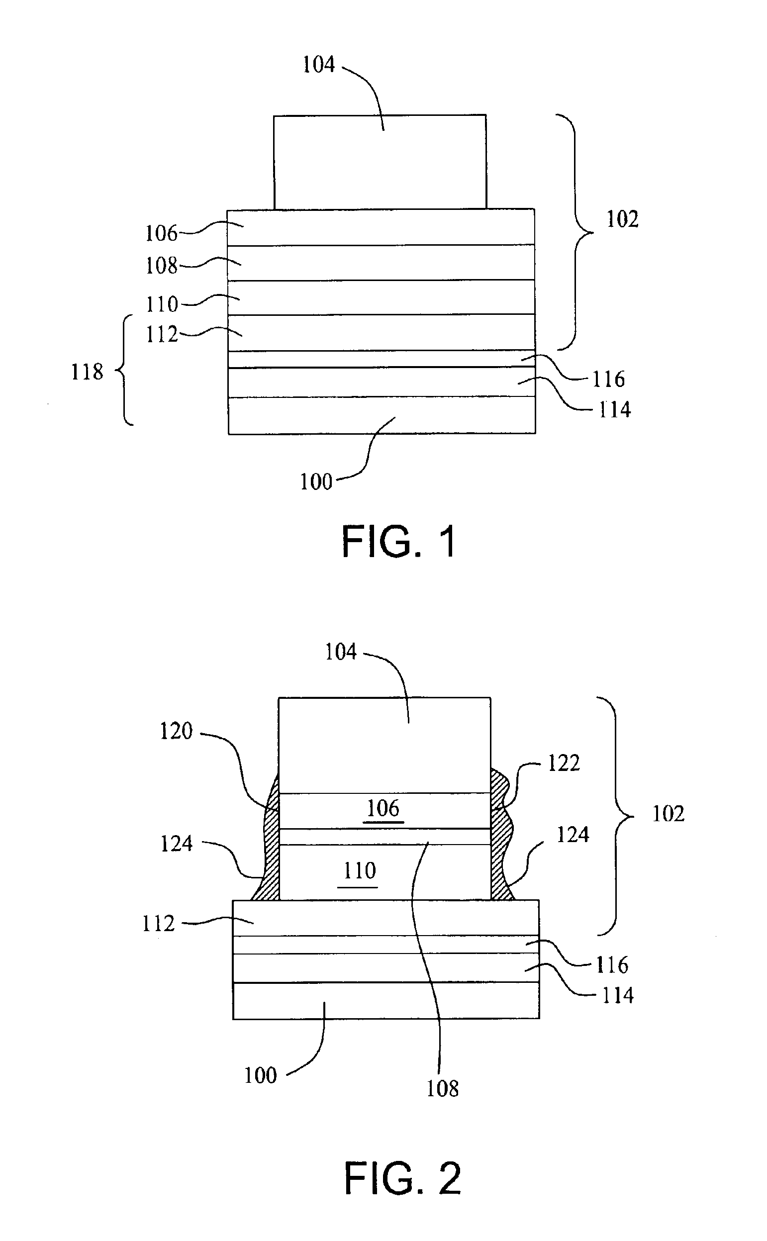
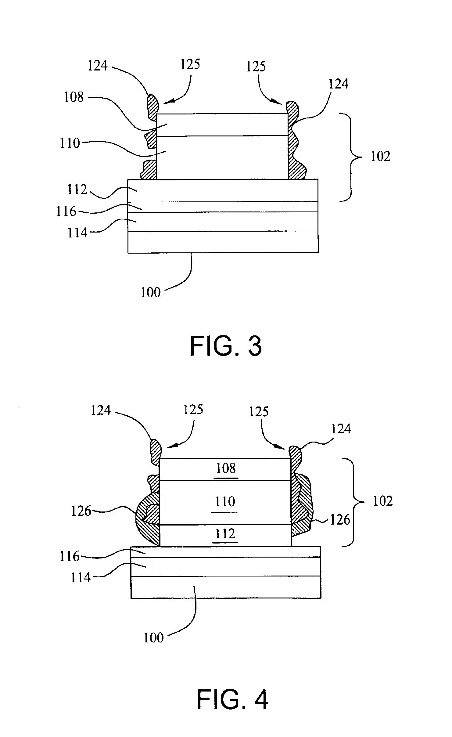
[0022]FIG. 1 is a schematic cross-sectional view of a substrate 100 before the photoresist str...
PUM
 Abstract
Description
Claims
Application Information