Semiconductor chip and semiconductor package including the same

a semiconductor and chip technology, applied in the direction of semiconductor devices, semiconductor/solid-state device details, electrical apparatus, etc., can solve the problems of marked decrease of manufacturing yield, and frequent electrical short circuits, so as to prevent or at least minimize the occurrence of short circuits

Active Publication Date: 2011-05-26
SK HYNIX INC
View PDF8 Cites 35 Cited by
  • Summary
  • Abstract
  • Description
  • Claims
  • Application Information

AI Technical Summary

Benefits of technology

[0014]An embodiment of the present invention is directed to a semiconductor chip which can prevent or at least minimize the occurrence of a short circuit when stacking semiconductor chips using through-silicon vias, and a semiconductor package including the same.

Problems solved by technology

However, in the course of electrically connecting the stacked semiconductor chips, unwanted portions of the upper semiconductor chip and the lower semiconductor chip may become electrically short-circuited, whereby electrical short circuits frequently occur.
When conducting the reflow process, the melted junction metals are likely to flow onto the lower surface of the upper semiconductor chip along the exposed portions of the through-silicon vias, so that the unwanted portions of the upper semiconductor chip and the lower semiconductor chip are electrically short-circuited, whereby electrical short circuits frequently occur.
If the short circuits occur, misoperation of the semiconductor chip is caused, whereby the manufacturing yield can markedly decrease.
While a process for applying an insulating material to the lower surface of the semiconductor chip can be additionally conducted to prevent the occurrence of a short circuit, processing difficulties are caused when attempting to apply the insulation material only to the lower surface of the semiconductor chip while exposing the electrically connected portions, and the processing time and processing cost increase.

Method used


Image

  • Semiconductor chip and semiconductor package including the same
  • Semiconductor chip and semiconductor package including the same
  • Semiconductor chip and semiconductor package including the same

Examples


Embodiment Construction

[0040]Hereafter, specific embodiments of the present invention will be described in detail with reference to the accompanying drawings.

[0041]It is to be understood herein that the drawings are not necessarily to scale and in some instances proportions may have been exaggerated in order to more clearly depict certain features of the invention. It should be noted that directions and references (e.g., upper surface, lower surface, top, bottom, etc.) may be used to facilitate the discussion of the drawings and are not intended to restrict the breadth of application of the claims presented.

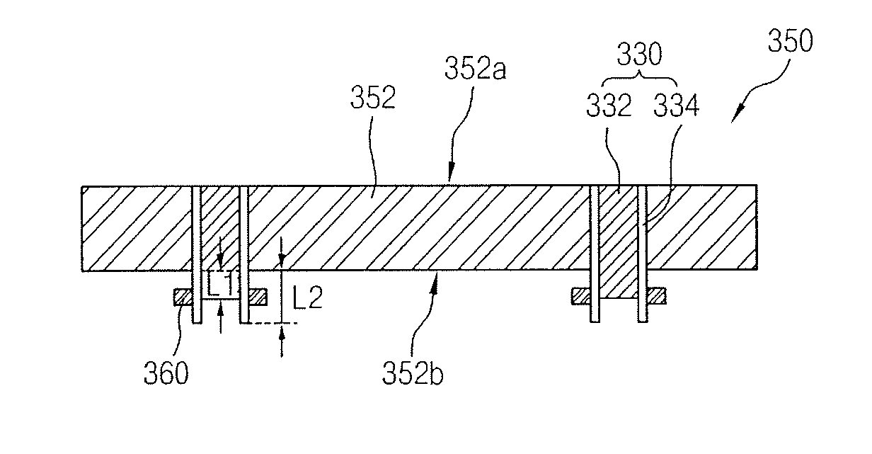
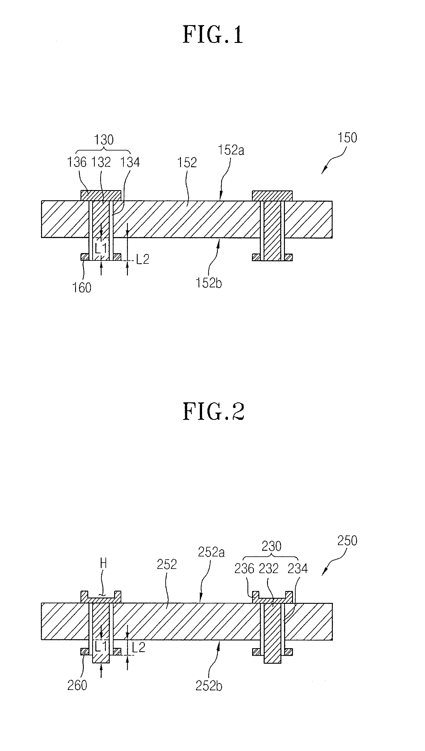
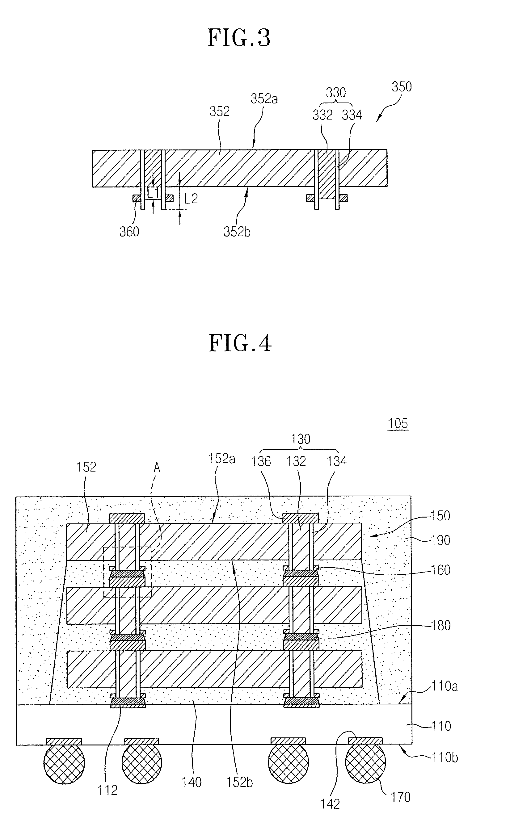
[0042]FIG. 1 is a cross-sectional view showing a semiconductor chip in accordance with an embodiment of the present invention. FIG. 2 is a cross-sectional view showing a semiconductor chip in accordance with another embodiment of the present invention. FIG. 3 is a cross-sectional view showing a semiconductor chip in accordance with another embodiment of the present invention.

[0043]Referring to FIG. 1, ...


PUM


Abstract

A semiconductor chip includes a semiconductor chip body, a through-silicon via and a silicon pattern. The semiconductor chip body has a first surface and a second surface facing away from the first surface. The through-silicon via is formed to pass through the semiconductor chip body and has a metal layer and an insulation layer which protrude from the second surface. The silicon pattern is formed on a sidewall of the protruding through-silicon via.

Description

CROSS-REFERENCE TO RELATED APPLICATIONS[0001]The present application claims priority to Korean patent application number 10-2009-0112621 filed on Nov. 20, 2009, which is incorporated herein by reference in its entirety.BACKGROUND OF THE INVENTION[0002]The present invention relates generally to a semiconductor chip and a semiconductor package including the same, and more particularly, to a semiconductor chip having through-silicon vias and a semiconductor package including the same.[0003]In the semiconductor industry, packaging technologies for integrated circuits are continuously being developed to satisfy the demand toward miniaturization and mounting reliability. For example, the demand toward miniaturization has resulted in the development of techniques for implementing a package with a size approaching that of a chip, and the demand toward mounting reliability has highlighted the importance of packaging techniques for improving the efficiency of mounting work and mechanical and ...

Claims


Application Information

Patent Timeline
Patent Type & Authority Applications(United States)
IPC IPC(8): H01L23/48
CPCH01L21/563H01L23/3128H01L2224/131H01L23/481H01L24/03H01L24/13H01L24/16H01L25/0657H01L2224/10126H01L2224/13099H01L2224/16145H01L2224/73203H01L2225/06513H01L2225/06541H01L2924/14H01L2924/15311H01L2924/3025H01L2924/01033H01L2924/014H01L2224/0401H01L2924/181
Inventor KIM, SEONG CHEOL
Owner SK HYNIX INC
Why Eureka
Try Eureka