Display device

a display device and display panel technology, applied in static indicating devices, instruments, photoelectric discharge tubes, etc., can solve the problems of mechanical strength required for operating the display device, display panel is easily smudged, display quality might be deteriorated, etc., to achieve mechanical strength, easy smudging, and improved display quality

Active Publication Date: 2011-05-26
SEMICON ENERGY LAB CO LTD
View PDF47 Cites 15 Cited by
  • Summary
  • Abstract
  • Description
  • Claims
  • Application Information

AI Technical Summary

Benefits of technology

[0006]In the case of a display device including such a touch sensor described above as an input device, a display panel of the display device keeps being touched by an object. Accordingly, the display panel is easily smudged and display quality might be deteriorated. Further, the mechanical strength needed for operating the display device is required. Furthermore, display device users are easily tired when the display panel of the display device is hard.

Problems solved by technology

Accordingly, the display panel is easily smudged and display quality might be deteriorated.
Further, the mechanical strength needed for operating the display device is required.
Furthermore, display device users are easily tired when the display panel of the display device is hard.

Method used


Image

  • Display device
  • Display device
  • Display device

Examples


embodiment 1

[0029]In this embodiment, a display device is described with reference to FIG. 1, FIG. 2, FIG. 3, FIG. 4, FIG. 5, and FIG. 6.

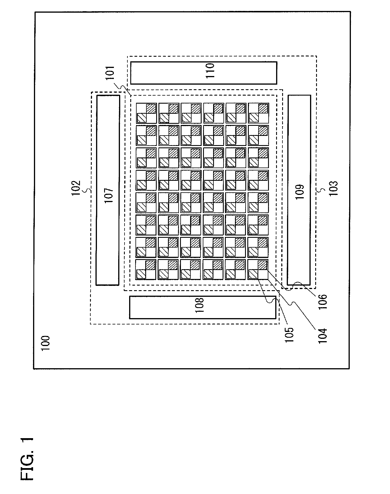
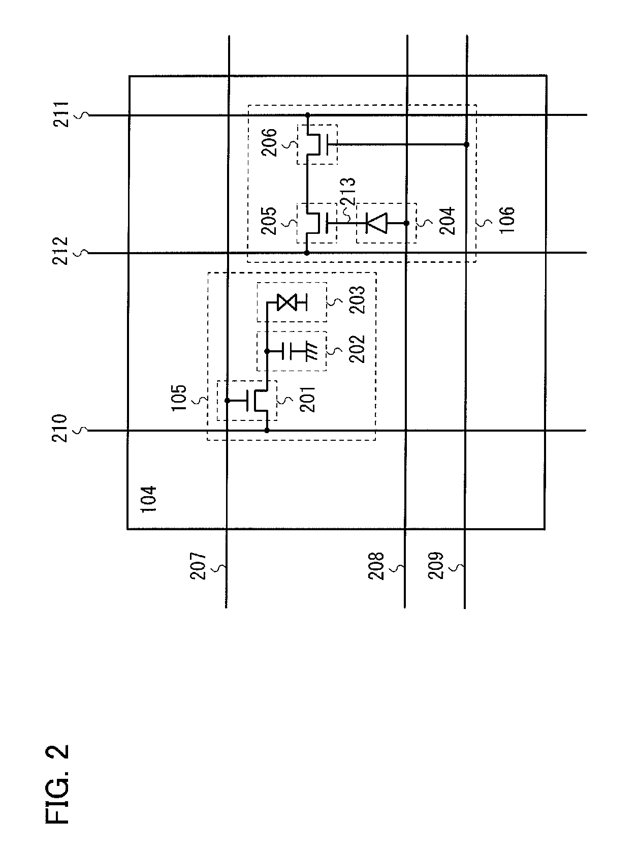
[0030]The structure of a display panel will be described with reference to FIG. 1. A display panel 100 includes a pixel circuit 101, a display element control circuit 102, and a photosensor control circuit 103. The pixel circuit 101 includes a plurality of pixels 104 arranged in matrix of rows and columns. Each of the pixels 104 includes a display element 105 and a photosensor 106. Note that the photosensor 106 may be provided outside the pixel 104. Further, the number of photosensors 106 may be different from that of display elements 105.

[0031]Each of the display elements 105 includes a thin film transistor (TFT), a storage capacitor, a liquid crystal element, and the like. The thin film transistor has a function of controlling injection or discharge of charge to / from the storage capacitor. The storage capacitor has a function of holding charge which correspo...

embodiment 2

[0060]FIG. 7 illustrates an example of a cross-sectional view of the display panel. In the display panel in FIG. 7, a photodiode 1002, a transistor 1003, a storage capacitor 1004, and a liquid crystal element 1005 are provided over a substrate (TFT substrate) 1001 having an insulating surface.

[0061]The photodiode 1002 and the storage capacitor 1004 can be formed at the same time as the transistor 1003 is formed in a manufacturing process of the transistor 1003. The photodiode 1002 is a lateral junction pin diode. A semiconductor film 1006 included in the photodiode 1002 has a region having p-type conductivity (p-type layer), a region having i-type conductivity (i-type layer), and a region having n-type conductivity (n-type layer). Note that although the case where the photodiode 1002 is a pin diode is illustrated in this embodiment, the photodiode 1002 may be a pn diode. Lateral pin junction or lateral pn junction can be formed in such a manner that an impurity imparting p-type cond...

embodiment 3

[0081]FIG. 8 illustrates an example of a cross-sectional view of a display panel different from that in Embodiment 2. In the display panel illustrated in FIG. 8, the photodiode 1002 differs from that in FIG. 7 in having a shielding film 2019 formed using a conductive film 1019 that is used for a gate electrode of the transistor 1003. By the shielding film in the photodiode 1002, light from the backlight can be prevented from directly entering a region that is intrinsic (i-type layer) and only light reflected off an object can be efficiently detected.

[0082]Further, in the case where the photodiode 1002 serves as a lateral pin diode, a region that has p-type conductivity (a p-type layer) and a region that has n-type conductivity (n-type layer) can be formed by self-aligned process using the shielding film as a mask. This is effective in manufacturing a small photodiode, in reducing the pixel size, and in improving the aperture ratio.

[0083]By employing such a mode, a display panel in w...


PUM


Abstract

A purpose is to enable detection of an object in a display device including a display panel provided with photosensors when the object touches the display panel and when the object does not touch the display panel. A display device includes a display panel provided with photosensors. The display device has a function of detecting an object with the photosensor when the object touches the display panel and when the object does not touch thereto. The display device has a function of changing the sensitivity of the photosensor varies depending on whether the object touches the display panel.

Description

BACKGROUND OF THE INVENTION[0001]1. Field of the Invention[0002]The present invention relates to a display device including a photosensor and a driving method of the display device. In particular, the present invention relates to a display device in which pixels each provided with a photosensor are arranged in matrix and to a driving method of the display device. Further, the present invention relates to an electronic device including the display device. In addition, the present invention relates to a semiconductor device and a driving method thereof.[0003]2. Description of the Related Art[0004]In recent years, a display device provided with a touch sensor has attracted attention. The display device provided with a touch sensor is called a touch panel, a touch screen, or the like (hereinafter referred to simply as a touch panel). Examples of the touch sensor include a resistive touch sensor, a capacitive touch sensor, and an optical touch sensor which are different in operation prin...

Claims


Application Information

Patent Timeline
Patent Type & Authority Applications(United States)
IPC IPC(8): G06F3/042H01J40/14
CPCG06F3/0412G09G3/20G06F3/042
Inventor KUROKAWA, YOSHIYUKI
Owner SEMICON ENERGY LAB CO LTD
Why Eureka
Try Eureka