Solar Cell Element, Color Sensor and Method of Manufacturing Light Emitting Element and Light Receiving Element

a technology of solar cells and light emitting elements, applied in the direction of solid-state devices, sustainable manufacturing/processing, final product manufacturing, etc., can solve the problem that conventional solar cell elements are incapable of sufficiently absorbing incident ligh

Inactive Publication Date: 2011-06-02
HONDA MOTOR CO LTD +1
View PDF6 Cites 58 Cited by
  • Summary
  • Abstract
  • Description
  • Claims
  • Application Information

AI Technical Summary

Problems solved by technology

The inventors made studies about causes of failure to obtain a sufficiently high power generation efficiency in conventional solar cell elements having semiconductor nanorods and knew that the conventional solar cell elements were incapable of sufficiently absorbing incident light in some cases.

Method used


Image

  • Solar Cell Element, Color Sensor and Method of Manufacturing Light Emitting Element and Light Receiving Element
  • Solar Cell Element, Color Sensor and Method of Manufacturing Light Emitting Element and Light Receiving Element
  • Solar Cell Element, Color Sensor and Method of Manufacturing Light Emitting Element and Light Receiving Element

Examples


first embodiment

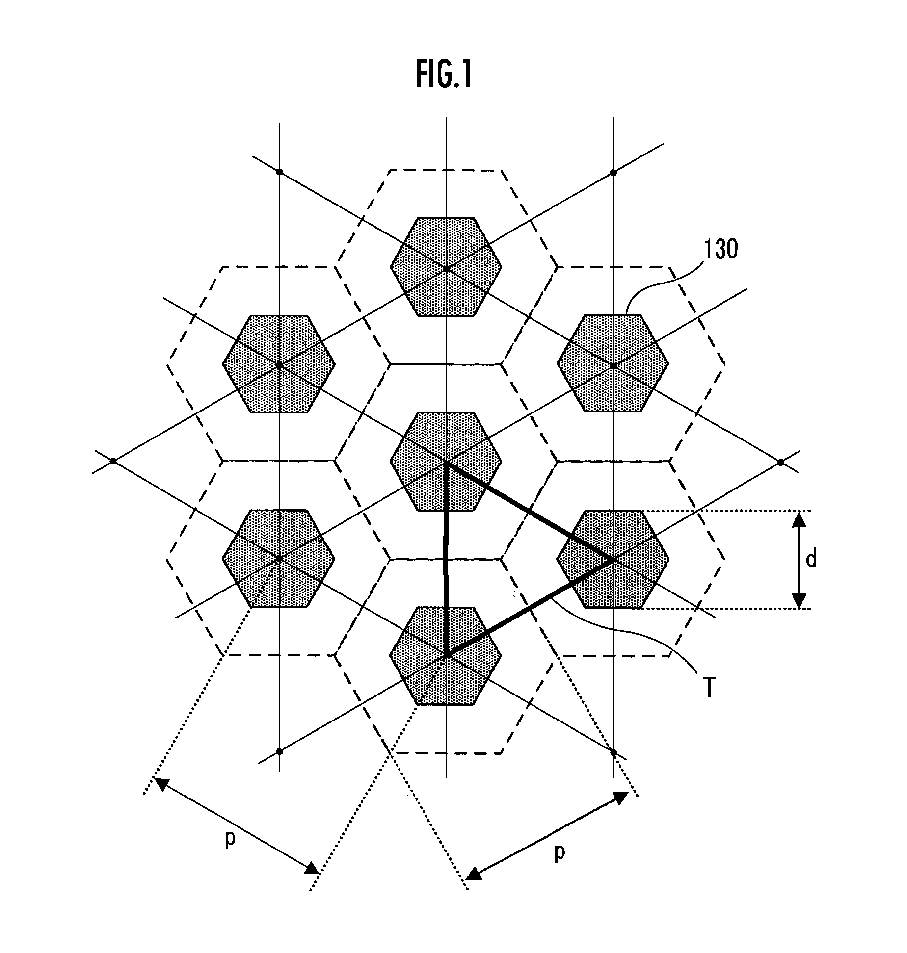
[0159]In a first embodiment of the present invention, an example of a semiconductor nanorod array used in the solar cell element of the present invention is illustrated.

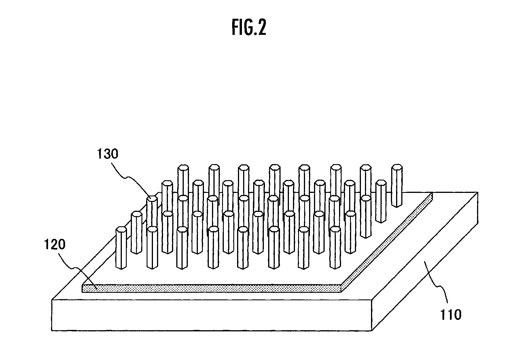
[0160]FIG. 1 is a perspective view showing the construction of the semiconductor nanorod array in the first embodiment. As shown in FIG. 1, the semiconductor nanorod array in the first embodiment has an electroconductive GaAs(111)B substrate 110, an amorphous SiO2 film 120 and semiconductor nanorods130.

[0161]A method of manufacturing the semiconductor nanorod array shown in FIG. 1 will be described.

[0162]First, the GaAs(111)B substrate 110 is cleaned and the amorphous SiO2 film 120 is formed to a thickness of about 20 nm on the surface of the GaAs(111)B substrate 110 by using an RF sputtering apparatus with a SiO2 target.

[0163]Next, a positive resist is applied on the amorphous SiO2 film 120; the GaAs(111)B substrate 110 is set in an EB drawing apparatus; and a pattern in which circular holes are arrayed in triangula...

second embodiment

[0174]In a second embodiment of the present invention, an example of a solar cell element of the present invention having a plurality of quantum well layers is illustrated.

[0175]FIG. 4 is a perspective view showing the construction of the solar cell element in the second embodiment. As shown in FIG. 4, a solar cell element 100 in the second embodiment has an electroconductive GaAs substrate 110, a silicon oxide (SiO2) film 120, semiconductor nanorods 130, a transparent embedment film 140, a transparent electrode 150, a first metal electrode 160 and a second metal electrode 170. The first electrode 160 and the second electrode 170 are connected to an external circuit.

[0176]The electroconductive GaAs substrate 110 is an electroconductive GaAs(111)B substrate.

[0177]The SiO2 film 120 covers the (111)B plane of the GaAs substrate 110. The film thickness of the SiO2 film 120 is, for example, 20 nm. In regions of the SiO2 film 120 where the semiconductor nanorods 130 are disposed, openings...

third embodiment

[0193]While in the second embodiment an example of the solar cell element of the present invention having quantum well layers is illustrated, an example of a solar cell element of the present invention further having a surface protective layer is illustrated in a third embodiment of the present invention.

[0194]The solar cell element in the third embodiment is identical in construction to the solar cell element 100 in the second embodiment shown in FIG. 4 except that the construction of the semiconductor nanorods is different. Description will therefore be made by reading a solar cell element 100′ in the third embodiment in place of the solar cell element 100 in the second element, and semiconductor nanorods 130′ in place of the semiconductor nanorods 130 in FIG. 4. The components identical to those of the solar cell element 100 in the second embodiment are indicated by the same reference numerals, and the description of the portions appearing again will not be repeated.

[0195]As show...


PUM


Abstract

A solar cell element having improved power generation efficiency is provided. A solar cell element 100 has a substrate 110, a mask pattern 120, semiconductor nanorods 130, a first electrode 150 and a second electrode 160. The semiconductor nanorods 130 are disposed in triangular lattice form as viewed in plan on the substrate 110. The ratio p / d of the center-to-center distance p between each adjacent pair of the semiconductor nanorods 130 and the minimum diameter d of the semiconductor nanorods 130 is within the range from 1 to 7. Each semiconductor nanorod 130 has a central nanorod 131 formed of a semiconductor of a first conduction type, a first cover layer 132 formed of an intrinsic semiconductor and covering the central nanorod 131, and a second cover layer 138 formed of a semiconductor of a second conduction type and covering the first cover layer 132.

Description

[0001]This application claims the foreign priority benefit under 35 U.S.C. §119 of Japanese Patent Application No. 2009-272140 filed on Nov. 30, 2009, and Japanese Patent Application No. 2010-261564 filed on Nov. 24, 2010, respectively, the disclosures of which are incorporated herein by reference.BACKGROUND OF THE INVENTION[0002]1. Field of the Invention[0003]The present invention relates to a solar cell element and a color sensor each having semiconductor nanorods and to a method of manufacturing a light emitting element and a light receiving element each having semiconductor nanorods.[0004]2. Description of the Related Art[0005]1. Solar Cell Element[0006]Solar cell elements having semiconductor nanorods (nanowires) are capable of increasing the surface area with respect to incident light and are, therefore, thought to be superior to thin-film solar cell elements in power generation efficiency. In recent years, several reports have been made of solar cell elements having semicondu...

Claims


Application Information

Patent Timeline
Patent Type & Authority Applications(United States)
IPC IPC(8): H01L31/06H01L31/18H01L31/0352B82Y20/00H01L31/0725H01L31/0735H01L31/075H01L31/076H01L31/10H01L33/08H01L33/24H01L33/32
CPCB82Y20/00Y02E10/548H01L21/02455H01L21/02505H01L21/02513H01L21/02538H01L21/02603H01L21/0262H01L27/14607H01L27/153H01L31/03048H01L31/035209H01L31/035218H01L31/035227H01L31/035236H01L31/035281H01L31/03529H01L31/075H01L31/076H01L31/184H01L31/1848H01L33/06H01L33/08H01L33/24H01L33/18Y02E10/544H01L21/0237Y02P70/50
Inventor GOTO, HAJIMEENDO, HIROTAKAHIRUMA, KENJIMOTOHISA, JUNICHIFUKUI, TAKASHI
Owner HONDA MOTOR CO LTD
Why Eureka
Try Eureka