Method of manufacturing organic light emitting display apparatus, surface treatment device for organic light emitting display apparatus, and organic light emitting display apparatus

Active Publication Date: 2011-06-02
SAMSUNG DISPLAY CO LTD
View PDF7 Cites 22 Cited by
  • Summary
  • Abstract
  • Description
  • Claims
  • Application Information

AI Technical Summary

Benefits of technology

[0010]The present embodiments provide a method of manufacturing an organic light emitting display apparatus whereby an organic emissive layer ma

Problems solved by technology

If the organic emissive layers are not formed in the desired corresponding sub-pixels, but in other sub-pixels, the organic emissive layers emit visible rays of mixed colors, thereby lowering image quality of an organic light emitting display apparatus.
W

Method used


Image

  • Method of manufacturing organic light emitting display apparatus, surface treatment device for organic light emitting display apparatus, and organic light emitting display apparatus
  • Method of manufacturing organic light emitting display apparatus, surface treatment device for organic light emitting display apparatus, and organic light emitting display apparatus
  • Method of manufacturing organic light emitting display apparatus, surface treatment device for organic light emitting display apparatus, and organic light emitting display apparatus

Examples


Embodiment Construction

[0034]The present embodiments will now be described in more detail in terms of features and operations with reference to the accompanying drawings.

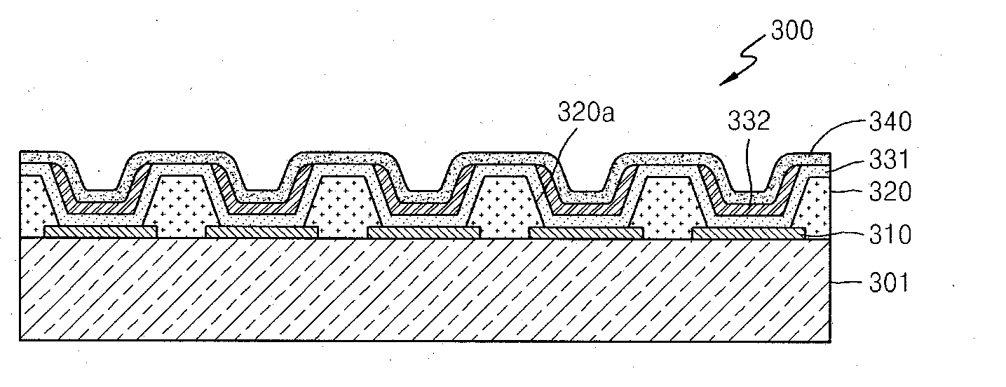
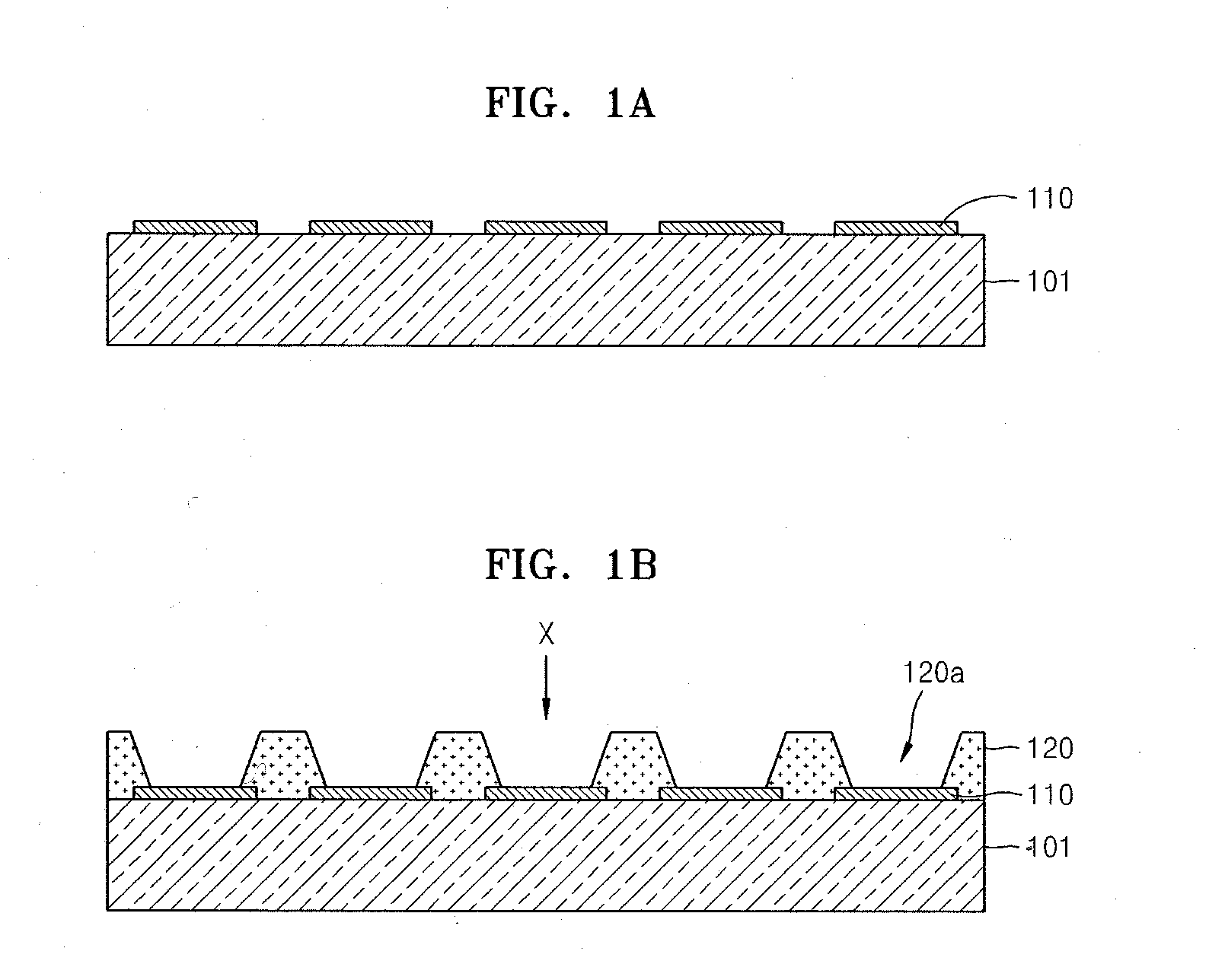
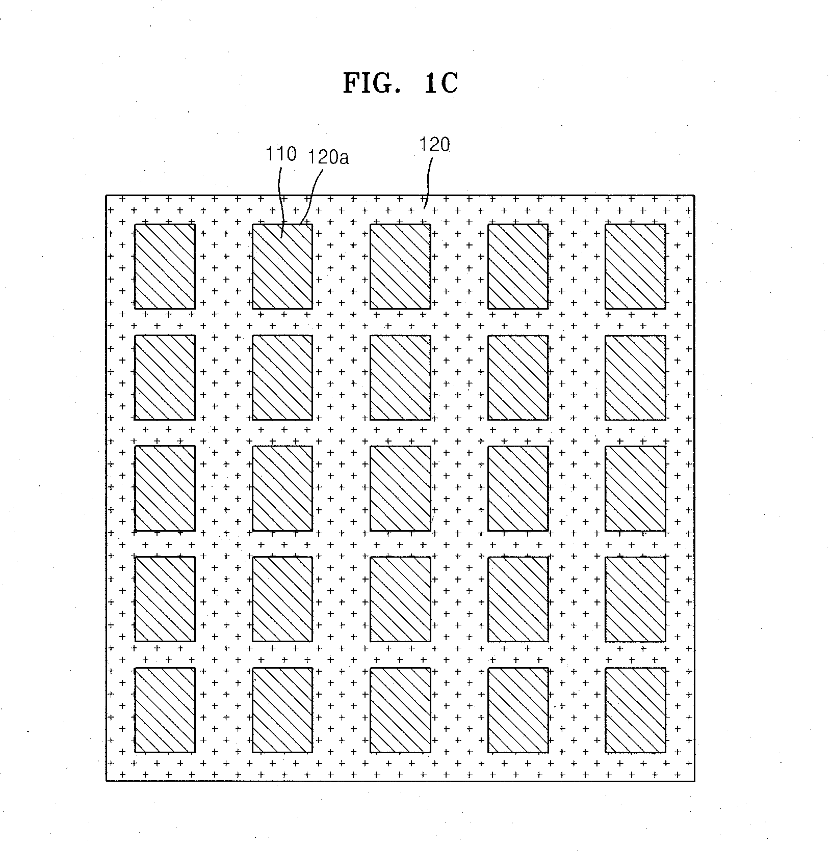
[0035]FIGS. 1A through 1G are cross-sectional views sequentially illustrating a method of manufacturing an organic light emitting display apparatus 100, according to an embodiment.

[0036]Referring to FIG. 1A, first electrodes 110 are formed on a substrate 101. Before the formation of the first electrodes 110, a thin-film transistor (TFT) may be formed on the substrate 101. The method of the present embodiment may be used in manufacturing an active matrix organic light emitting display apparatus and a passive matrix organic light emitting display apparatus.

[0037]The substrate 101 comprises, for example, a transparent glass material including SiO2 as a main component. However, the substrate 101 is not limited thereto, and may comprise, for example, a transparent plastic material. A plastic substrate may comprise, for example, an insulating o...


PUM


Abstract

Provided are a method of manufacturing an organic light emitting display apparatus, a surface treatment device for an organic light emitting display apparatus, and an organic light emitting display apparatus. To easily form organic emissive layers, the method includes: forming a first electrode on a substrate; forming on the first electrode a pixel defining layer having openings that expose predetermined portions of the first electrode; forming a charge carrying layer on the pixel defining layer and the first electrode exposed through the openings; hydrophobically treating portions of a surface of the charge carrying layer selectively, wherein the portions do not correspond to the openings, using a laser; forming organic emissive layers on the charge carrying layer; and forming a second electrode on the organic emissive layers so as to be electrically connected with the organic emissive layers.

Description

CROSS-REFERENCE TO RELATED APPLICATIONS[0001]This application claims the benefit of Korean Patent Application No. 10-2009-0115921, filed on Nov. 27, 2009, in the Korean Intellectual Property Office, the disclosure of which is incorporated herein in its entirety by reference.BACKGROUND OF THE INVENTION[0002]1. Field of the Invention[0003]The present embodiments relate to a method of manufacturing an organic light emitting display apparatus, a surface treatment device for an organic light emitting display apparatus, an organic light emitting display apparatus, a method of manufacturing an organic light emitting display apparatus whereby an organic emissive layer may easily be formed, a surface treatment device for an organic light emitting display apparatus, and an organic light emitting display apparatus.[0004]2. Description of the Related Art[0005]Portable thin film type flat panel display devices have been widely used. Among flat panel display apparatuses, electroluminescent displa...

Claims


Application Information

Patent Timeline
IPC IPC(8): H01L51/00H01L21/28G21K5/00
CPCH01L21/268H01L51/0012H01L51/0004H01L27/3283H10K59/173H10K71/13H10K71/191H05B33/10H10K71/00
Inventor CHOI, EUN-SUNKIM, WON-YONGNAM, MYENG-WOOPARK, JIN-HANKIM, SUNG-GONKIM, JOON-HYUNG
Owner SAMSUNG DISPLAY CO LTD
Why Eureka
Try Eureka