Enhancing mosfet performance by optimizing stress properties

Inactive Publication Date: 2011-06-02
ALSEPHINA INNOVATIONS INC
View PDF13 Cites 13 Cited by
  • Summary
  • Abstract
  • Description
  • Claims
  • Application Information

AI Technical Summary

Benefits of technology

[0007]A device and method for improving performance of a transistor includes gate structures formed on a substrate having a spacing therebetween. The gate structures are formed in an operative relationship with active areas formed in the substrate. A stress liner is formed on the gate structures. An ang

Problems solved by technology

Stress liners with the same stress polarity do not usually provide maximum

Method used


Image

  • Enhancing mosfet performance by optimizing stress properties
  • Enhancing mosfet performance by optimizing stress properties
  • Enhancing mosfet performance by optimizing stress properties

Examples


Embodiment Construction

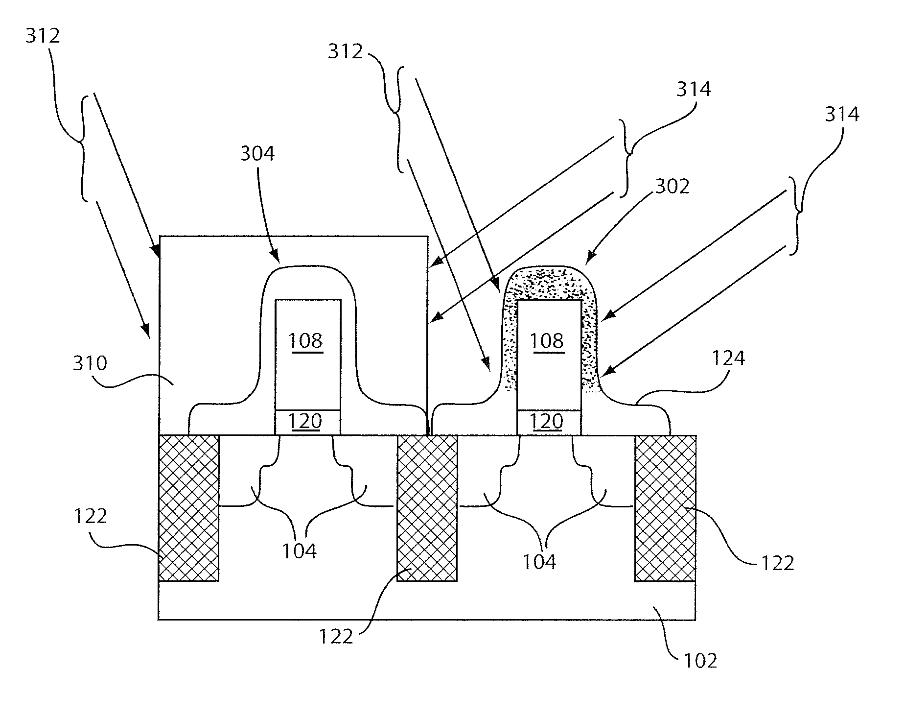
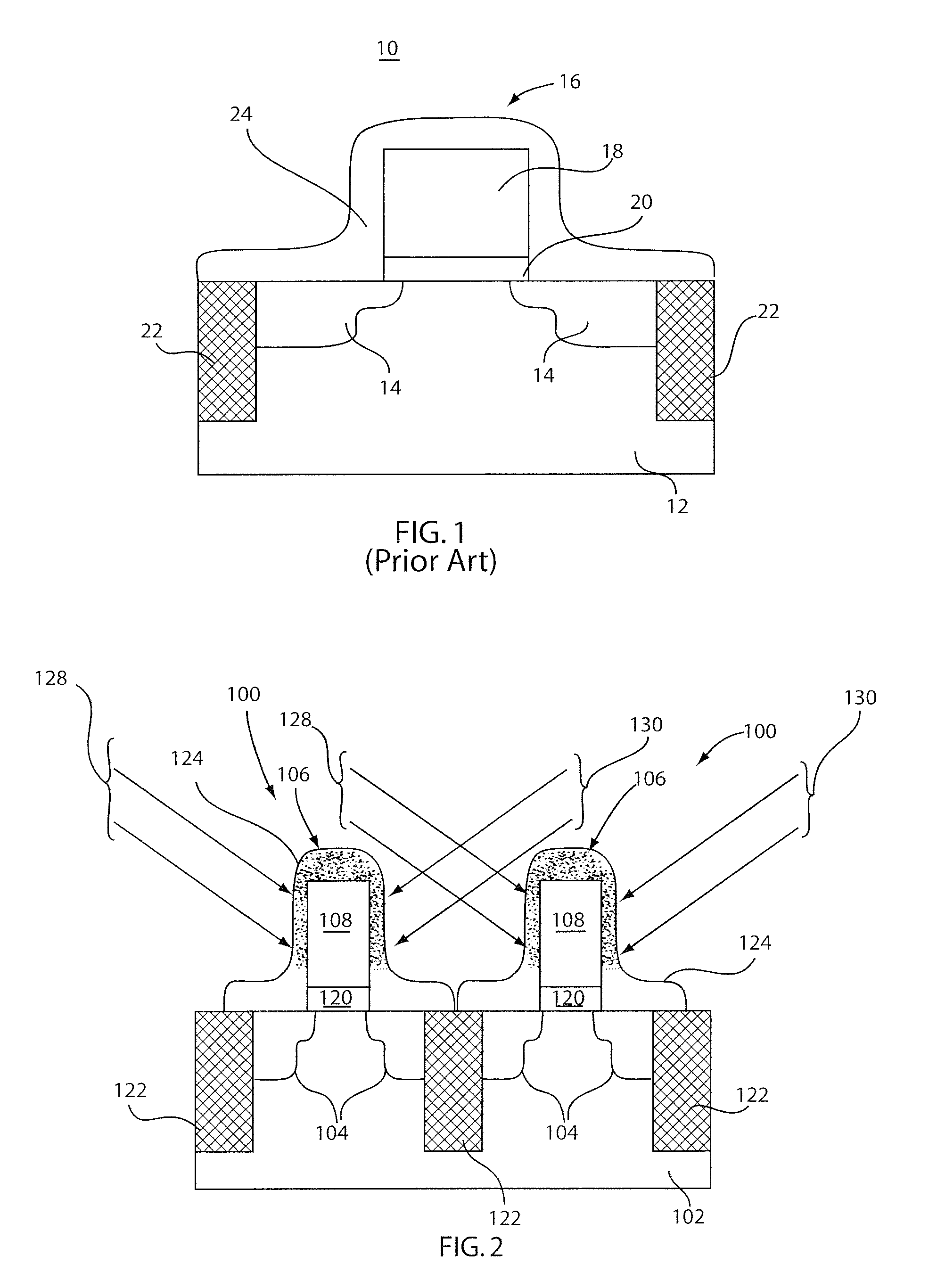
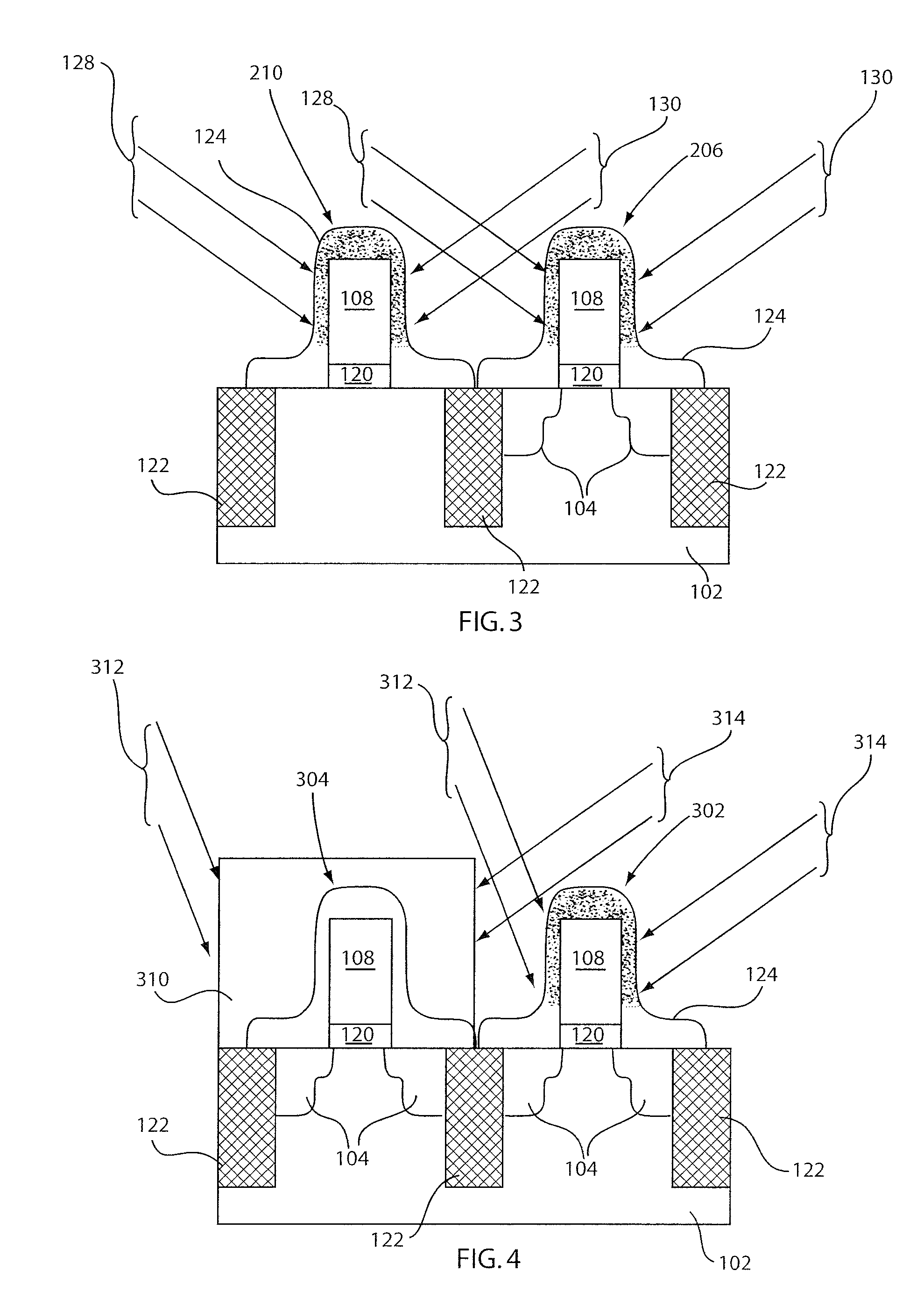
[0016]In accordance with the present principles, stress liners are processed to adjust stress conditions and to improve device performance. Depending on the device type (e.g., N-type field effect transistors (NFETs) or P-type field effect transistors (PFETs)), the stress magnitudes, the direction of the stress, the type stress (e.g., tensile or compressive) and / or the position of the stress can be adjusted to permit improved device performance.

[0017]In FET devices, a relationship exists between carrier mobility (μ) and stress (σ). This relationship may be expressed as

Δμμ≈πxσx+πyσy+πzσz(1)

where μ is carrier mobility; π is a piezoresistive coefficient and σ is stress; x, y and z subscripts indicate coordinates.

[0018]For an illustrative NFET and PFET in silicon, a standard {001} surface with a notch along provided the following parameters in Table 1:

TABLE 1DirectionSi Piezoresistive Coefficient, πCurrentStress, σNFETPFETX-directionX (longitudinal)(π11 + π12 + π44)−31.671.8X-directionY...


PUM


Abstract

A device and method for improving performance of a transistor includes gate structures formed on a substrate having a spacing therebetween. The gate structures are formed in an operative relationship with active areas fainted in the substrate. A stress liner is formed on the gate structures. An angled ion implantation is applied to the stress liner such that ions are directed at vertical surfaces of the stress liner wherein portions of the stress liner in contact with the active areas are shielded from the ions due to a shadowing effect provided by a height and spacing between adjacent structures.

Description

BACKGROUND[0001]1. Technical Field[0002]The present invention relates to semiconductor fabrication, and more particularly to field effect transistors having stress relieved stress liners to improve performance.[0003]2. Description of the Related Art[0004]Stress liners are extensively used to boost metal oxide semiconductor field effect transistor (MOSFET) performance. An as-deposited stress liner has the same stress polarity in all directions (i.e., either tensile or compressive in all directions). Stress liners with the same stress polarity do not usually provide maximum performance gain.[0005]Referring to FIG. 1, a simplified cross-sectional view of a MOSFET 10 is shown. The MOSFET 10 is formed in a semiconductor substrate 12. The substrate 12 includes source and drain regions (S / D) 14, which include dopants to create active areas. The S / D regions 14 permit conduction when enabled by an activated gate 16. The gate includes a gate conductor 18 isolated from the substrate 12 by a ga...

Claims


Application Information

Patent Timeline
IPC IPC(8): H01L29/78H01L21/336
CPCH01L21/26586H01L21/31155H01L21/823807H01L29/7843H01L29/6659H01L29/7833H01L21/823864
Inventor CHENG, KANGGUODORIS, BRUCE B.ZHANG, YING
Owner ALSEPHINA INNOVATIONS INC
Why Eureka
Try Eureka