Stacked Display With A Bended Substrate, An Electronic Apparatus And A Method For Manufacturing The Same

a technology of stacked display and bended substrate, which is applied in the manufacture of electrode systems, electric discharge tubes/lamps, instruments, etc., can solve the problems of large plurality of pixels that have to be matched optically and geometrically, difficulty in ensuring alignment accuracy, so as to prevent the damage of interconnect regions , the overall size of the display stack is minimized , the effect of improving alignment accuracy

Inactive Publication Date: 2011-06-02
SAMSUNG ELECTRONICS CO LTD
View PDF10 Cites 20 Cited by
  • Summary
  • Abstract
  • Description
  • Claims
  • Application Information

AI Technical Summary

Benefits of technology

[0004]It is an object of the invention to provide a stack display wherein interconnect problems are relieved. It is a further object of the invention to provide a stack display wherein alignment problems between different display layers forming the stack are substantially mitigated.
[0037]It is found to be advantageous to provide radiation transmissive markers for enabling due alignment of the stack during a manufacturing step of the stack display according to the invention. Preferably, the marker comprises a light transparent region which may be suitably detected in a light transmission set-up. More preferable, each said region comprises at least one said marker. By matching two markers, each on one of the regions to be aligned, the alignment accuracy is substantially improved.

Problems solved by technology

It is a disadvantage of the known stack color display that a great plurality of pixels have to be matched optically and geometrically.
In particular, for active-matrix stacked color displays alignment problems constitute a substantial handicap, as every pixel of a given primary color in the panel needs to be matched correctly with the two pixels of the complementary primary colors at the same position in the stack.
More in particular, it is a disadvantage of the known stack display that a number of interconnect problems persist when stacking a number of display layers on top of each other.

Method used


Image

  • Stacked Display With A Bended Substrate, An Electronic Apparatus And A Method For Manufacturing The Same
  • Stacked Display With A Bended Substrate, An Electronic Apparatus And A Method For Manufacturing The Same
  • Stacked Display With A Bended Substrate, An Electronic Apparatus And A Method For Manufacturing The Same

Examples


Embodiment Construction

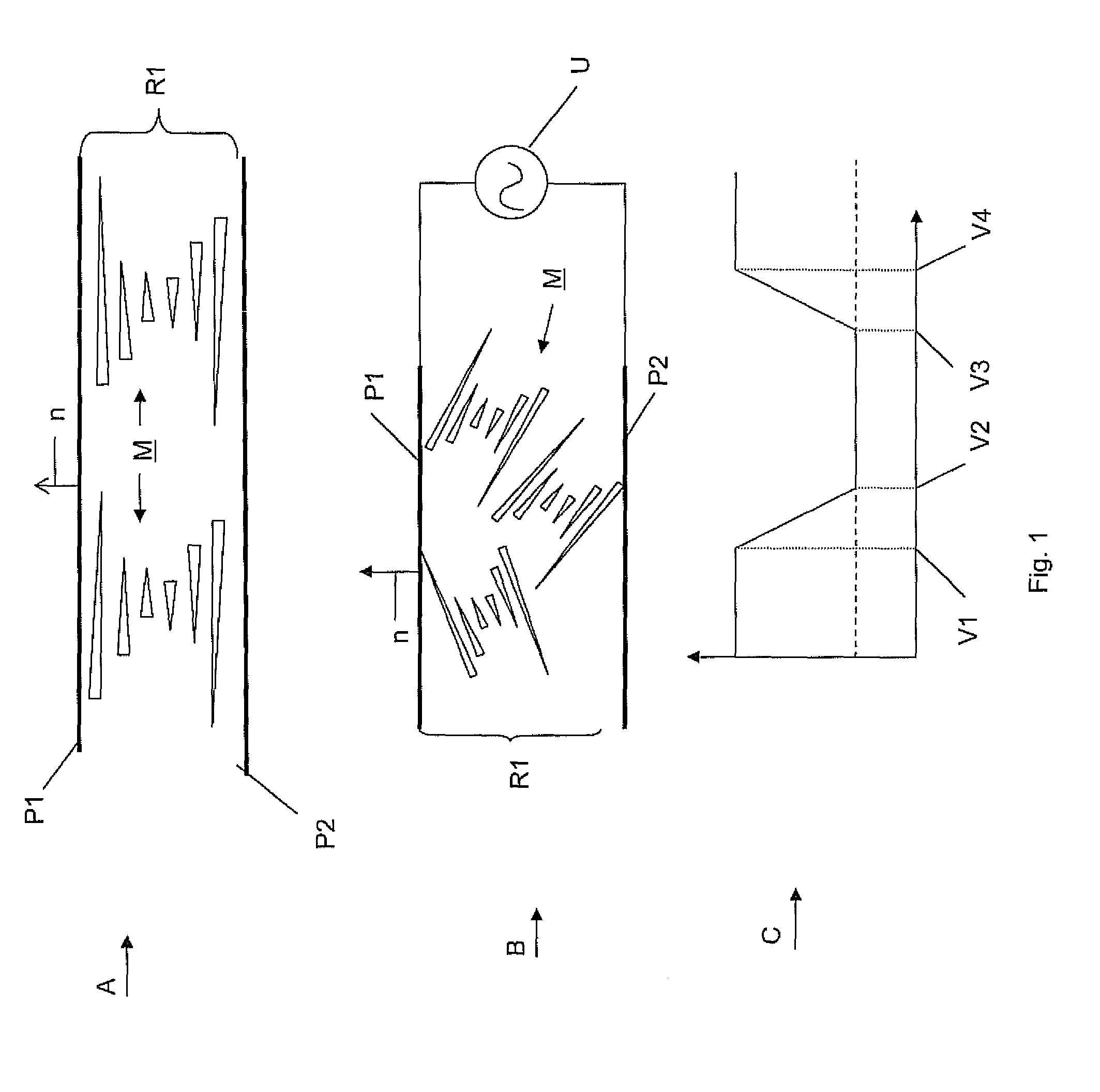
[0056]FIG. 1 presents an embodiment of a CLC material suitable for use in a stack color display according to an embodiment of the invention. A CLC color display may be based on chiral nematic CLC molecules confined between two parallel portions of a substrate (P1, P2) for defining a region (R1). By suitable substrate surface treatment, two liquid crystal phases exist (A, B) that may be stable at or near to room temperature. In absence of external electric field a planar phase (view A) may be enabled which comprise liquid crystal molecules (M) forming a helical structure with the helical axes lying predominantly parallel to the surface normal (n).

[0057]Application of a voltage pulse U to the region R1 can cause the cholesteric material to switch to the focal-conic texture. Here, the CLC structure may comprise small polydomain regions typically 10 μm wide. Within each domain there is planar structure, but the overall helix of each domain region is randomly oriented. A random distribut...


PUM

PropertyMeasurementUnit
diameteraaaaaaaaaa
diameteraaaaaaaaaa
reflectancesaaaaaaaaaa

Abstract

A stacked display (20b) comprises superposed regions for changing between a reflective color state (R, G, B) and a transparent state, which regions form part of a˜bended substrate (20). The substrate (20) may comprise a sequence of portions (1-6) which forms regions having pre-defined color. Each portion (1-6) is electrically connected to a further portion in the sequence by interconnect regions (b′, c′, d′) which form an oversized loop between the regions (1-2, 3-4, 5-6) when the substrate (20) is bent. The regions (1-2, 3-4, 5-6) are filled with a suitable optoelectronic color material (R, G, B).

Description

FIELD[0001]The invention relates to a stacked display. In particular, the invention relates to a cholesteric liquid crystal (CLC) display, electrowetting display or a stack display combining any two or more display technologies, wherein a display layer may be alternated between a color state and a transmissive state. The invention further relates to a method of manufacturing a stack display. The invention further relates to an electronic apparatus comprising a stack display.BACKGROUND[0002]An embodiment of a stack color display is known from US2002 / 0135719 A1, which operates using a cholesteric liquid crystal (CLC) principle. The known CLC display comprises first and second substrates facing and being spaced apart from each other. Beneath the first substrate a first transparent electrode is positioned, whereas a light absorbing layer is positioned on a second substrate. A CLC color filter layer is positioned on the light absorption layer, which comprises a multi-layer structure, eac...

Claims


Application Information

Patent Timeline
Patent Type & Authority Applications(United States)
IPC IPC(8): G09G5/00H05K3/00
CPCG02B5/201G02B5/3016G02B26/004G02B26/005G02F1/133305Y10T29/49124G02F1/13718Y10T29/4913Y10T156/1026Y10T156/1044Y10T156/1046G02F1/13473
Inventor HUITEMA, HJALMAR EDZER AYCOVAN LIESHOUT, PETRUS JOHANNES GERARDUSVAN VEENENDAAL, ERIK
Owner SAMSUNG ELECTRONICS CO LTD
Why Eureka
Try Eureka