Mold release film for manufacturing semiconductor resin package and semiconductor resin package manufacturing method using same

a semiconductor resin and release film technology, applied in the direction of synthesized resin layered products, light beam reproducing, instruments, etc., can solve the problems of reducing work efficiency, shortening mold life, increasing the likelihood of generating burrs on etc., to improve the releasability of the semiconductor resin package, reduce the likelihood of warpage and wrinkles, and improve the effect of dimensional accuracy

Inactive Publication Date: 2011-06-09
MITSUI CHEM INC
View PDF3 Cites 18 Cited by
  • Summary
  • Abstract
  • Description
  • Claims
  • Application Information

AI Technical Summary

Benefits of technology

[0033]The present invention can provide a mold release film that offers excellent semiconductor resin package releasability as well as is less prone to warpage and wrinkling. Using the mold release film upon manufacturing of a semiconductor resin package, it is possible to provide a semiconductor resin package with good dimensional accuracy.

Problems solved by technology

The conventional transfer molding technique has the disadvantages of: 1) reducing work efficiency; 2) shortening mold life; and 3) increasing the likelihood of generating burrs on the semiconductor resin package.
Shorter mold life is due to the wear on the mold inner surface.
However, it is difficult with this approach to provide a semiconductor resin package of desired shape because PTFE films tend to develop wrinkles when placed in the mold cavity.
Moreover, PTFE films have the drawback of being difficult to dispose of as they generate fluorine gas when burned.

Method used


Image

  • Mold release film for manufacturing semiconductor resin package and semiconductor resin package manufacturing method using same
  • Mold release film for manufacturing semiconductor resin package and semiconductor resin package manufacturing method using same
  • Mold release film for manufacturing semiconductor resin package and semiconductor resin package manufacturing method using same

Examples


example 1

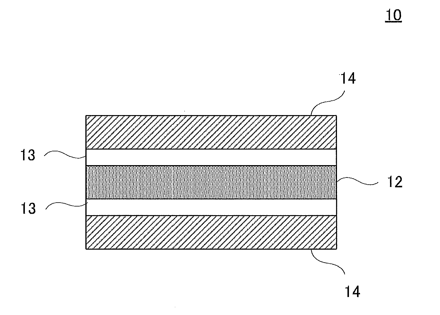
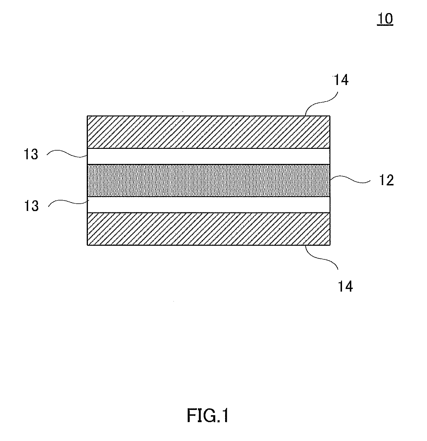
[0133]The above-described raw layer materials were co-extruded with a T-die molding machine to manufacture a non-stretched mold release film of 400 mm width. The mold release film had a 5-layer structure consisting of three different layers: A-1 / B-1 / C-1 / B-1 / A-1, wherein their thicknesses were 15 μm / 5 μm / 25 μm / 5 μm / 15 μm, respectively (total thickness=65 μm).

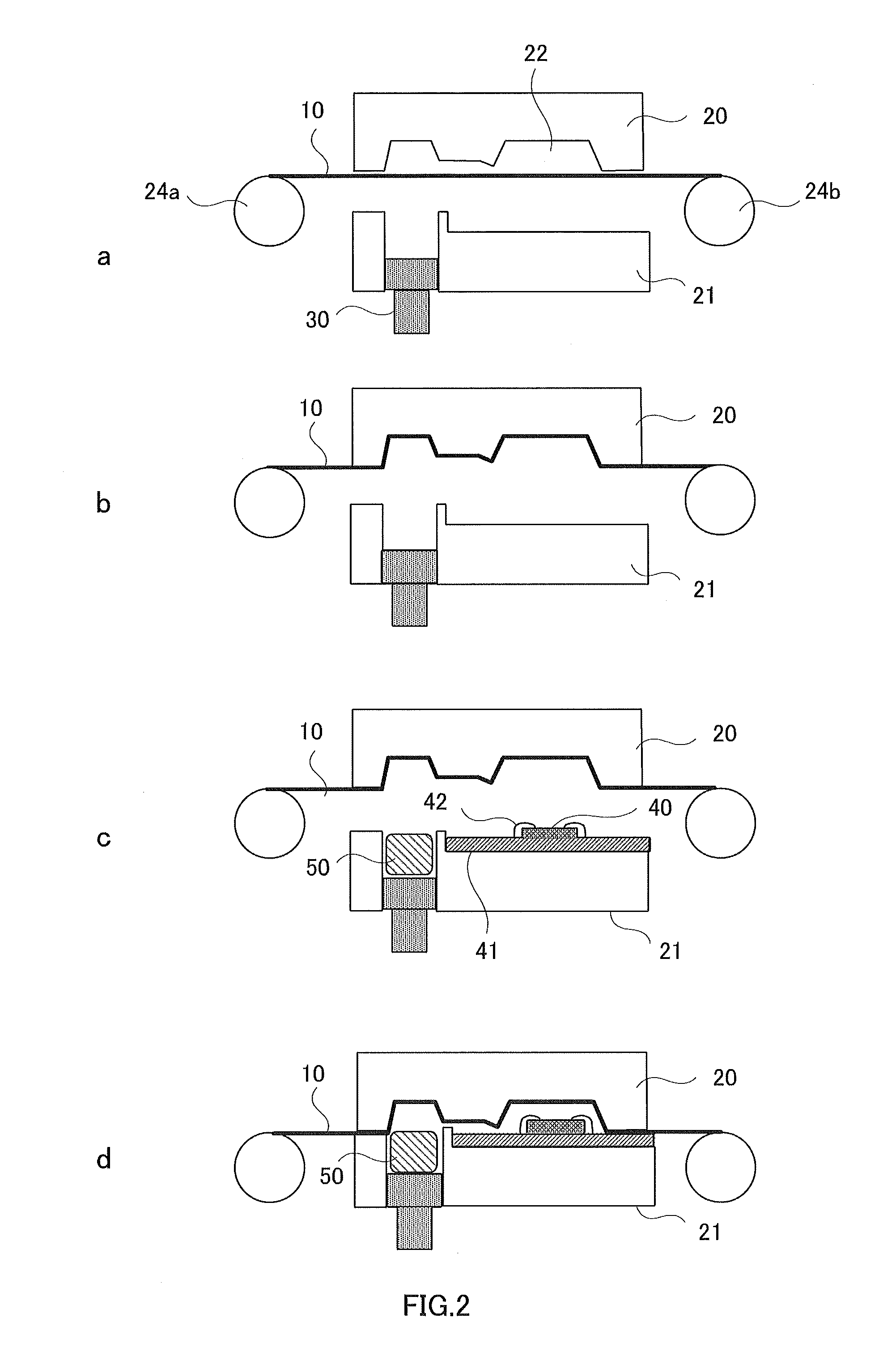
[0134]As illustrated in FIGS. 2a to 2d, obtained mold release film 10 was placed between upper mold 20 and lower mold 21. The depth of cavity 22 defined by upper mold 20 and lower mold 21, as measured from the mold parting surface, was 0.8 mm at the deepest point. The tensile applied to mold release film 10 by film feeding device 24a and film take-up device 24b was adjusted to a tensile strength of 1 MPa.

[0135]Mold release film 10 was then secured to the parting surface of upper mold 20 by vacuum suction as illustrated in FIG. 2b. Semiconductor chip 40 fixed to board 41 was placed onto lower mold 21 (see FIG. 2c), and then upper ...

example 2

[0169]Mold release film 10 was manufactured as in Example 1 except that the combination of layer thicknesses was set to 10 μm / 5 μm / 15 μm / 5 μm / 10 μm (total thickness=45 μm). Semiconductor resin package 61 was then manufactured using mold release film 10 and evaluated as in Example 1.

example 3

[0170]Mold release film 10 was manufactured as in Example 1 except that the combination of layer thicknesses was set to 10 μm / 5 μm / 20 μm / 5 μm / 10 μm (total thickness=50 μm). Semiconductor resin package 61 was then manufactured using mold release film 10 and evaluated as in Example 1.


PUM

PropertyMeasurementUnit
total thicknessaaaaaaaaaa
melting pointsaaaaaaaaaa
melting pointaaaaaaaaaa

Abstract

Provided are: a mold release film, which has excellent mold releasability to a semiconductor resin package and does not easily generate warpage, wrinkles and the like; and a method for obtaining a semiconductor resin package having excellent dimensional accuracy by using such mold release film. The mold release film for manufacturing a semiconductor resin package has one or more base material layers (C), a pair of outermost layers (A) which sandwich the base material layers (C) and contain a 4-methyl-1-pentene polymer as a main component, and a pair of adhesive layers (B) which adhere together the base material layers (C) and the outermost layers (A).

Description

TECHNICAL FIELD [0001]The present invention relates to mold release films for manufacturing semiconductor resin packages, and manufacturing methods of semiconductor resin packages using the same.BACKGROUND ART [0002]Semiconductor chips generally come in the form of semiconductor resin packages in which they are encapsulated with encapsulating material. A semiconductor resin package is generally manufactured by transfer molding wherein one or more semiconductor chips are placed in the cavity of a mold followed by filling of the entire cavity with an encapsulating material which contains epoxy resin as a main component. The conventional transfer molding technique has the disadvantages of: 1) reducing work efficiency; 2) shortening mold life; and 3) increasing the likelihood of generating burrs on the semiconductor resin package. Reduced work efficiency is attributed to the necessity to clean the mold, as encapsulating materials sometimes soil the mold inner surface. Shorter mold life ...

Claims


Application Information

Patent Timeline
Patent Type & Authority Applications(United States)
IPC IPC(8): H01L21/56B32B27/32B32B27/08B32B27/34B32B5/00
CPCB29C33/68B29C45/14655B32B7/12B32B27/08Y10T428/26B32B27/34H01L21/566H01L2224/48227H01L2924/1815B32B27/32Y10T428/31938Y10T428/3175Y10T428/31743C08F210/14H01L21/48
Inventor SANADA, TAKAYUKINORITOMI, KATSUMIMATAYOSHI, TOMOYA
Owner MITSUI CHEM INC
Why Eureka
Try Eureka