High Power Efficiency Polycrystalline CdTe Thin Film Semiconductor Photovoltaic Cell Structures for Use in Solar Electricity Generation

a solar cell, high-efficiency technology, applied in semiconductor/solid-state device manufacturing, semiconductor devices, electrical equipment, etc., can solve the problems of low power conversion efficiency of pv cells available in the art, low power conversion efficiency of light to electricity, and difficult or inconvenient continuous electrical energy supply, etc., to achieve high deposition rate polycrystalline growth, high performance, and high precision control of layer thickness

Inactive Publication Date: 2011-06-16
URIEL SOLAR
View PDF54 Cites 25 Cited by
  • Summary
  • Abstract
  • Description
  • Claims
  • Application Information

AI Technical Summary

Problems solved by technology

Photovoltaic cells can be used to power electrical equipment for which it has proven difficult or inconvenient to provide a source of continuous electrical energy.
There are PV cells available in the art, but these can be costly to produce.
In addition, PV cells available in the art might not provide high power conversion efficiency, from light to electricity, for a given quantity of light.

Method used


Image

  • High Power Efficiency Polycrystalline CdTe Thin Film Semiconductor Photovoltaic Cell Structures for Use in Solar Electricity Generation
  • High Power Efficiency Polycrystalline CdTe Thin Film Semiconductor Photovoltaic Cell Structures for Use in Solar Electricity Generation
  • High Power Efficiency Polycrystalline CdTe Thin Film Semiconductor Photovoltaic Cell Structures for Use in Solar Electricity Generation

Examples


Embodiment Construction

[0038]While various embodiments of the invention have been shown and described herein, it will be obvious to those skilled in the art that such embodiments are provided by way of example only. Numerous variations, changes, and substitutions will now occur to those skilled in the art without departing from the invention. It should be understood that various alternatives to the embodiments of the invention described herein may be employed in practicing the invention.

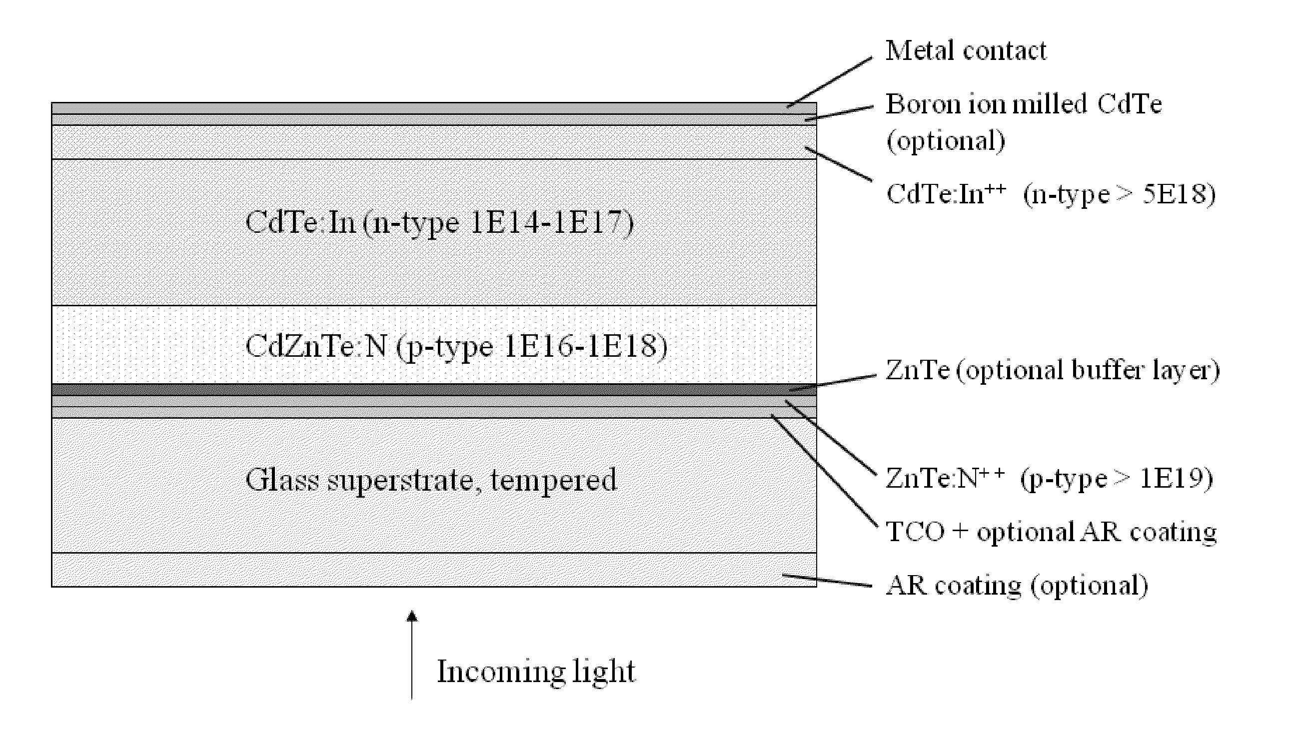
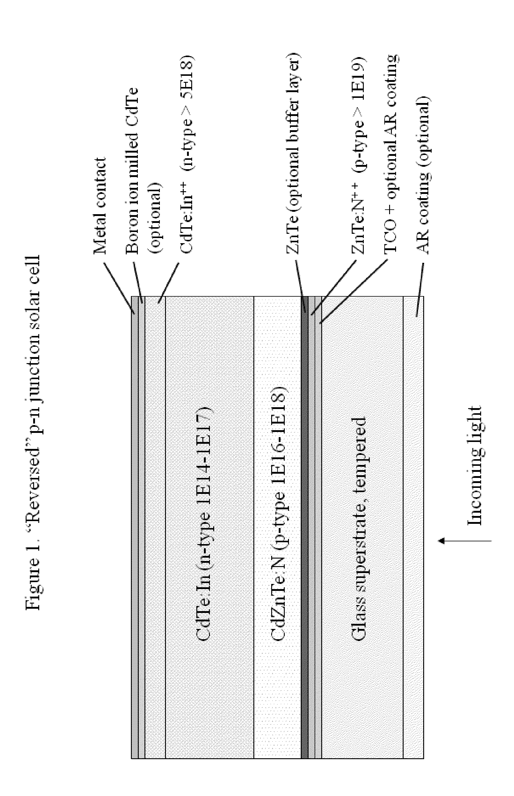
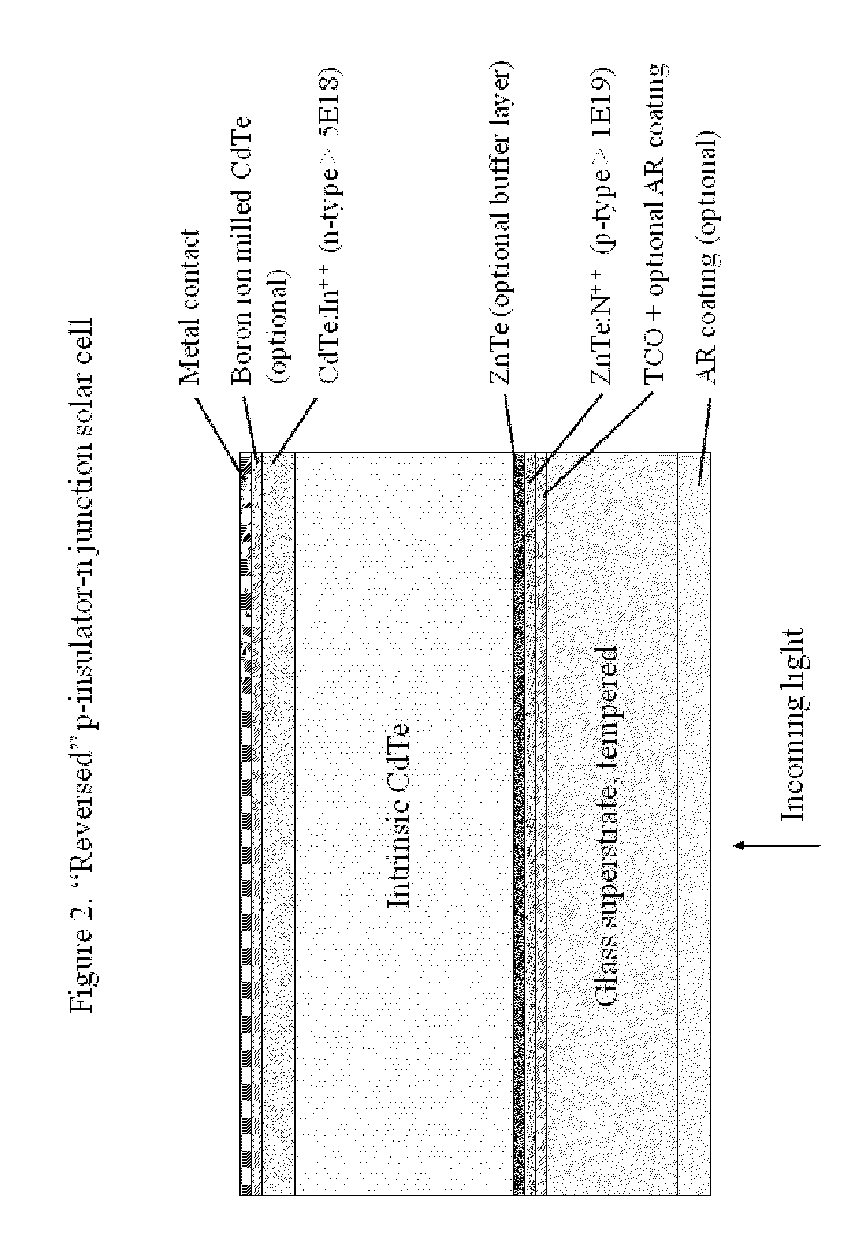
[0039]In current thin film photovoltaic cells, such as CdTe or CIGS, a CdS “window” layer is used because it is an intrinsically n-type material. Because current process technologies used in production do not provide the capability of doping photovoltaic structures in situ (i.e., real time in the deposition chamber), those of skill in the art use a material with high intrinsic n-type doping, such as CdS, to define the n-type layer of the p-n junction. But there are limitations associated with using CdS. For example, CdS (a...


PUM


Abstract

Solar cell structures formed using molecular beam epitaxy (MBE) that can achieve improved power efficiencies in relation to prior art thin film solar cell structures are provided. A reverse p-n junction solar cell device and methods for forming the reverse p-n junction solar cell device using MBE are described. A variety of n-p junction and reverse p-n junction solar cell devices and related methods of manufacturing are provided. N-intrinsic-p junction and reverse p-intrinsic-n junction solar cell devices are also described.

Description

CROSS-REFERENCE[0001]The application claims the benefit of U.S. Provisional Patent Application No. 61 / 285,531, filed Dec. 10, 2009, which is entirely incorporated herein by reference.FIELD OF THE INVENTION[0002]The invention relates to cadmium telluride (CdTe) thin film semiconductor solar cell structures, more particularly to high efficiency polycrystalline CdTe thin film semiconductor solar cell structures grown by molecular beam epitaxy (MBE).BACKGROUND OF THE INVENTION[0003]A photovoltaic cell is able to absorb radiant light energy and convert it directly into electrical energy. Some photovoltaic (“PV”) cells are employed as a measure of the ambient light in non-imaging applications or (in an array format) as imaging sensors in cameras to obtain an electrical signal for each portion of the image. Other photovoltaic cells are used to generate electrical power. Photovoltaic cells can be used to power electrical equipment for which it has proven difficult or inconvenient to provide...

Claims


Application Information

Patent Timeline
Patent Type & Authority Applications(United States)
IPC IPC(8): H01L31/0264H01L31/0256
CPCH01L21/02422H01L31/073H01L21/02502H01L21/02562H01L21/02573H01L21/02631H01L31/03925H01L31/065H01L31/075H01L31/1828H01L31/1832H01L31/1836Y02E10/543Y02E10/548H01L21/0248Y02E10/541
Inventor GARNETT, JAMES DAVIDDINGUS, PETERWANG, SHUMIN
Owner URIEL SOLAR
Why Eureka
Try Eureka