Radiation tolerant circuit for minimizing the dependence of a precision voltage reference from ground bounce and signal glitch

a voltage reference and ground bounce technology, applied in the field of voltage reference circuits, can solve the problems of affecting the performance of the whole adc, the possibility of correction, and the error of the replicated reference voltage (and current) and the direct impact of noise affecting the voltage referen

a voltage reference and ground bounce technology, applied in the field of voltage reference circuits, can solve the problems of affecting the performance of the whole adc, the possibility of correction, and the error of the replicated reference voltage (and current) and the direct impact of noise affecting the voltage referen

US20110148388A1Active Publication Date: 2011-06-23CAES COLORADO SPRINGS LLC

Image

  • Radiation tolerant circuit for minimizing the dependence of a precision voltage reference from ground bounce and signal glitch
  • Radiation tolerant circuit for minimizing the dependence of a precision voltage reference from ground bounce and signal glitch
  • Radiation tolerant circuit for minimizing the dependence of a precision voltage reference from ground bounce and signal glitch

Examples


Embodiment Construction

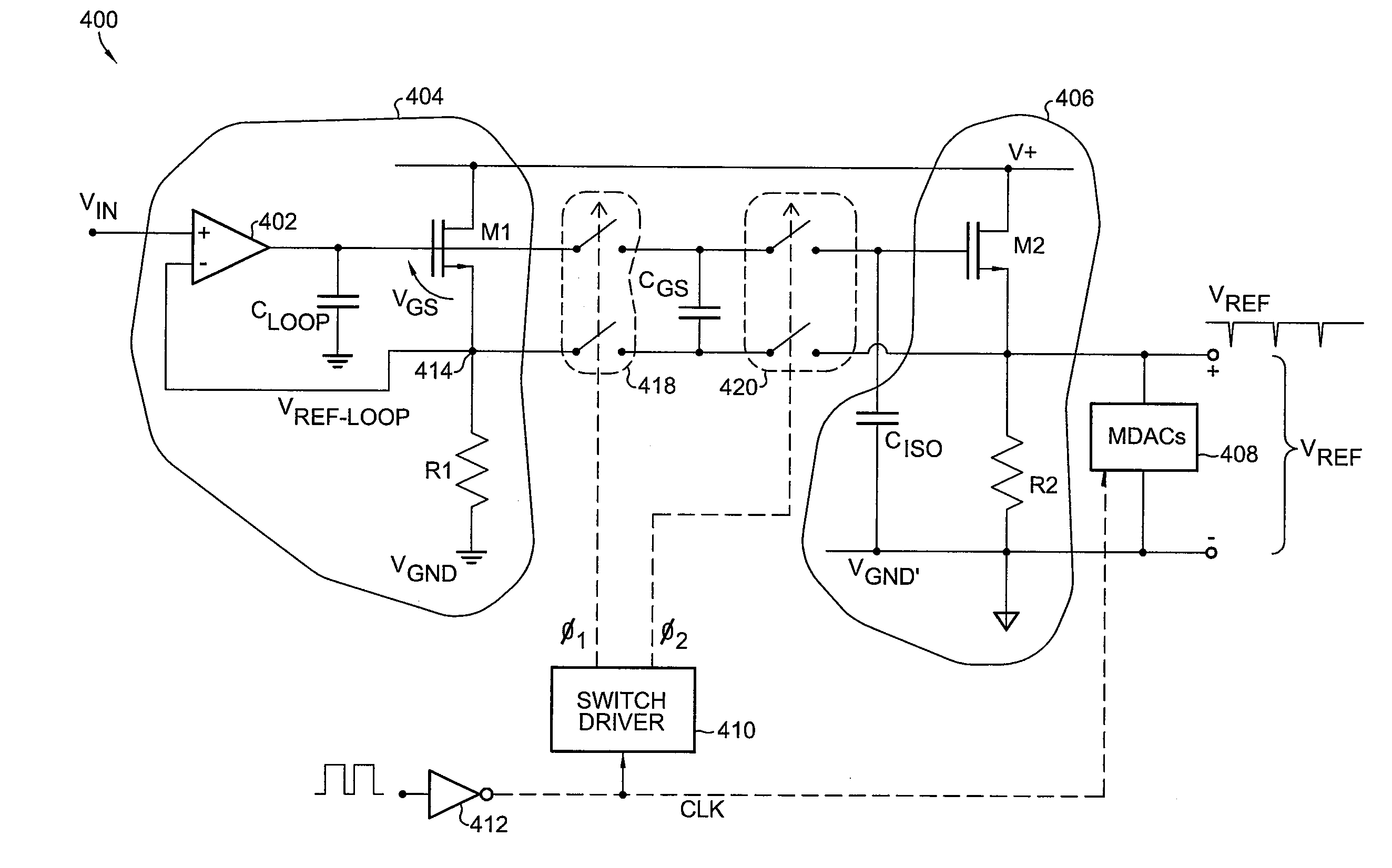
[0017]It is thus desirable to impart the wanted driving signal VREF=VREF—LOOP onto the MDACs of the ADC, without it being affected by any error existing between VGND and VGND′. This can be achieved by relying on the identity (or precision scaling) of the VGs of the follower's MOSFET and of the degeneration resistor, which were expected, and capitalized upon, also in prior art. In such case in fact, the VREF driver can be referenced to the precision loop by way of a floating (i.e., ground-independent) capacitor connected directly across the gate and source nodes of the active device, as illustrated in FIG. 4.

[0018]Referring now to FIG. 4, a reference circuit 400 according to the present invention is shown having an amplifier 402 having a positive input for receiving a VIN input signal, a negative input, and an output. A compensation capacitor CLOOP is coupled to the output of amplifier 402. The output of amplifier 402 is also coupled to the gate of transistor M1. The drain of transis...


PUM


Abstract

A radiation-hardened reference circuit includes a precision voltage reference circuit for generating a current-controlling voltage at first and second terminals, a driver circuit for receiving the current-controlling voltage at first and second terminals and for generating an output reference voltage, and a differential sampling circuit having first and second input terminals coupled to the first and second terminals of the voltage reference circuit, and first and second output terminals coupled to the first and second terminals of the driver circuit.

Description

FIELD OF THE INVENTION[0001]The present invention is related to voltage reference circuits and in particular to reducing noise and drift in voltage reference circuits that are used in switched-capacitor pipeline or SAR ADCs.BACKGROUND OF THE INVENTION[0002]Analog-to-digital conversion algorithms implemented in silicon (successive approximation registers or SARs, switched-capacitor and switched-current pipelines, folding, flash, etc.) inherently rely on the precision, accuracy, stability, and low noise of some internal reference voltage signal against which the input signals must be weighted. In particular, switched-capacitor implementations draw current out of the reference lines to charge / discharge the capacitors employed for processing the signal (in each stage's Multiplicative Digital-to-Analog Converter, or MDAC), usually perturbing the reference signal more than in switched-current implementations. For instance, the flash sub-ADC found in the first stage of a switched-capacitor...

Claims


Application Information

Patent Timeline
23 Jun 2011
Publication
US20110148388A1
IPC
G05F3/16
CPC
G11C27/026; G11C27/024; H02M3/158
Inventors
ZANCHI, ALFIO; HISANO, SHINICHI