Method and system for tracing die at unit level

a technology of tracing dies and units, applied in the field of tracing dies at unit level, can solve the problems of no longer being able to track historical wafer information related to each singulated die, no longer being able to use wafer maps,

Inactive Publication Date: 2011-06-30
STMICROELECTRONICS PTE LTD +1
View PDF6 Cites 23 Cited by
  • Summary
  • Abstract
  • Description
  • Claims
  • Application Information

AI Technical Summary

Problems solved by technology

Since the die are assigned new numbers based on the bins sort, the wafer map is no longer useful and tracking the die based on the wafer and lot is no longer carried out.
When the wafer are sawed into dice and packaged into individual units during the packaging proce

Method used


Image

  • Method and system for tracing die at unit level
  • Method and system for tracing die at unit level
  • Method and system for tracing die at unit level

Examples


Embodiment Construction

[0028]The making and using of embodiments are discussed in detail below. It should be appreciated, however, that specific embodiments discussed are merely illustrative, and do not limit the scope of the invention.

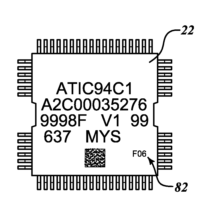
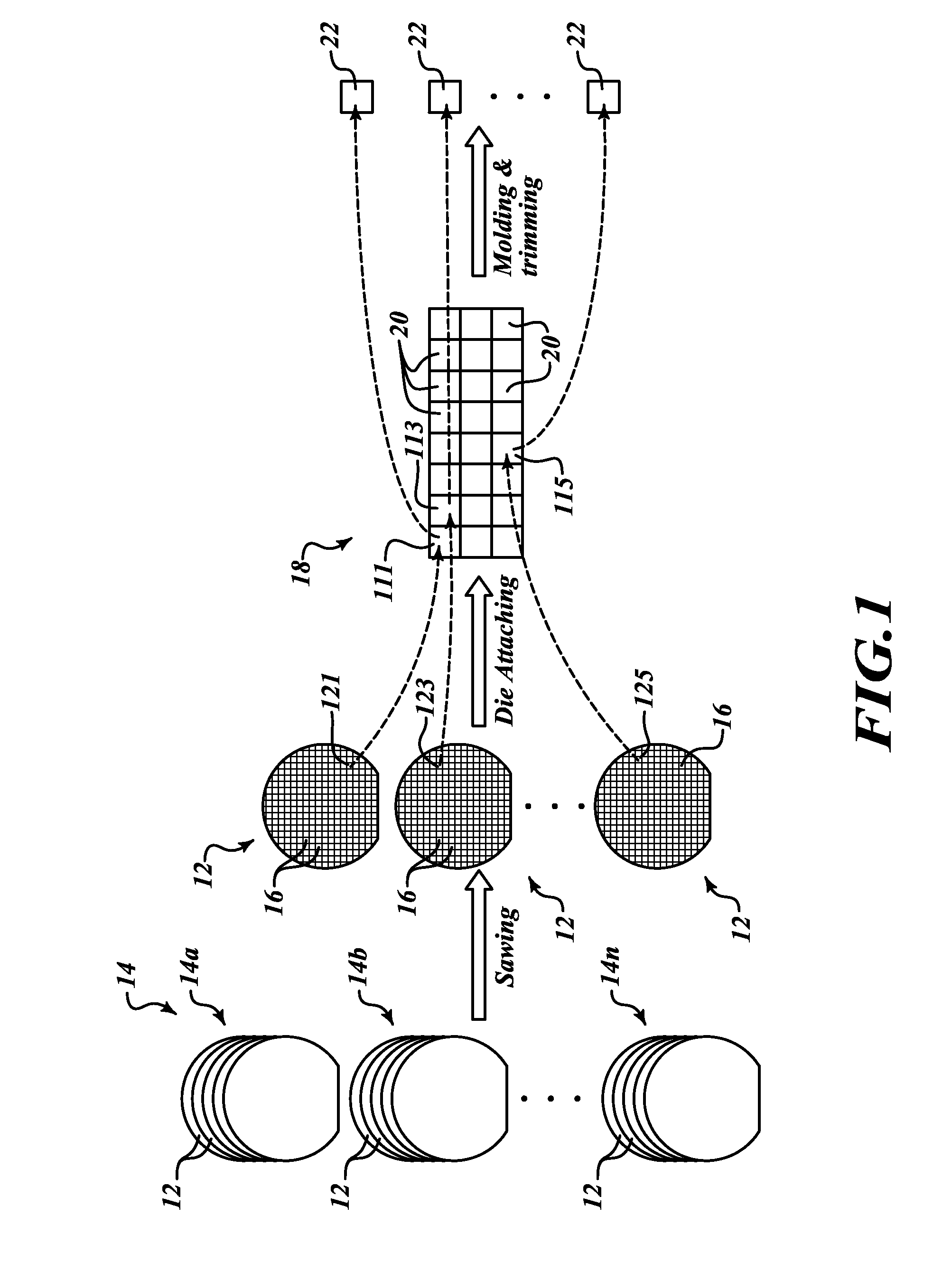
[0029]FIG. 1 illustrates schematically the process of manufacturing tested wafers into packaged dice where the wafers are sawed into dice 12 and then the dice 12 are picked and attached to a support member 11 and finally the support member 11 carrying the dice 12 is molded and trimmed into individual packaged dice 13.

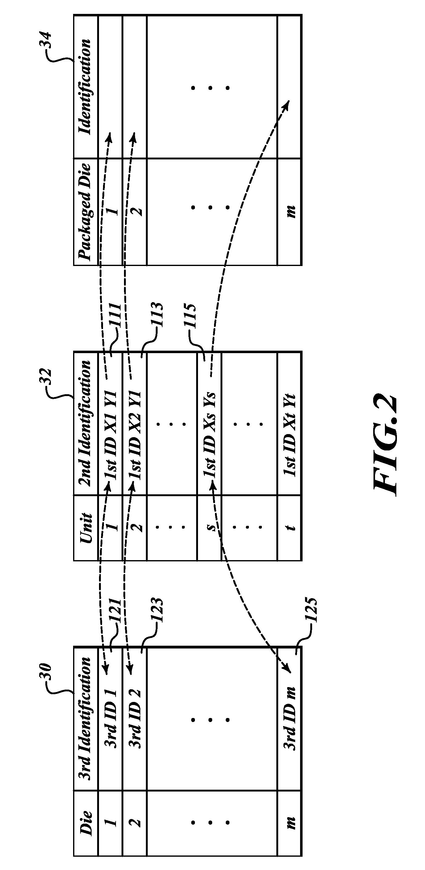
[0030]FIG. 1 is a schematic view of tracing die according to an embodiment. FIG. 1 shows a plurality of wafers 12 grouped according to respective lots 14. A first lot is labeled 14a, a second lot 14b, and subsequent lots 14n. Within each lot 14 are a plurality of wafers. For example, in lot 14a there may be 25 wafers in some front end technologies. In other manufacturing front ends, the lot size may vary from a small of one wafer per lot to in the range 10 to 2...


PUM


Abstract

A method and system for tracing die at unit level, comprising: assigning a first identification to a support member including a plurality of die support units; generating a second identification corresponding to a die support unit, the second identification including the first identification and a coordinate of the die support unit within the support member; correlating the second identification to a third identification of a die; attaching the die to the die support unit to generate a packaged die; and assigning the second identification to the packaged die.

Description

BACKGROUND[0001]1. Technical Field[0002]This invention relates generally to semiconductor and manufacturing methods thereof, and more particularly, but not exclusively, to tracking a unique identification to a dice after being singulated from a wafer and then marking this identification on the final package.[0003]2. Description of the Related Art[0004]A wafer undergoes many manufacturing processes to form many thousands of devices on it. During and after the manufacturing processes, the wafer is conventionally subjected to a series of testing procedures to confirm functionality of the devices, determine speed of operation, and assure quality and reliability. Data of the manufacturing processes and testing procedures are collected and stored in a database that identifies the wafer and each die on the wafer. Such data are stored in correlation with the wafer identification so that the process history and testing results of the devices on the wafer can be tracked as the wafer moves thr...

Claims


Application Information

Patent Timeline
IPC IPC(8): H01L23/544H01L21/56H01L21/50H01L21/66G06F17/30
CPCG01R31/26H01L2224/83H01L21/6835H01L23/544H01L24/16H01L24/32H01L24/81H01L24/83H01L2221/68372H01L2223/54406H01L2223/54433H01L2223/54473H01L2223/54486H01L2224/16225H01L2224/16245H01L2224/32225H01L2224/32245H01L21/568H01L21/67294H01L2924/14H01L2924/00
Inventor BINTANG, YOHANESNG, ENGHSIUNG
Owner STMICROELECTRONICS PTE LTD
Why Eureka
Try Eureka