Semiconductor memory device and method for writing data into flash memory

a memory device and memory technology, applied in the direction of memory address formation, memory allocation/allocation/relocation, instruments, etc., can solve the problems of page buffer double as saving buffer, difficult to improve the packing density of flash memory devices, etc., and achieve the effect of reducing the size of the ram

Active Publication Date: 2006-09-12
PANASONIC CORP
View PDF5 Cites 357 Cited by
  • Summary
  • Abstract
  • Description
  • Claims
  • Application Information

AI Technical Summary

Benefits of technology

[0010]An object of the present invention is to provide a semiconductor memory apparatus wherein the size of RAM is reduced

Problems solved by technology

However, improvements in packing density of the flash memory devices are not ea

Method used


Image

  • Semiconductor memory device and method for writing data into flash memory
  • Semiconductor memory device and method for writing data into flash memory
  • Semiconductor memory device and method for writing data into flash memory

Examples


Embodiment Construction

[0047]The following describes the best embodiment of the present invention, referring to the figures.

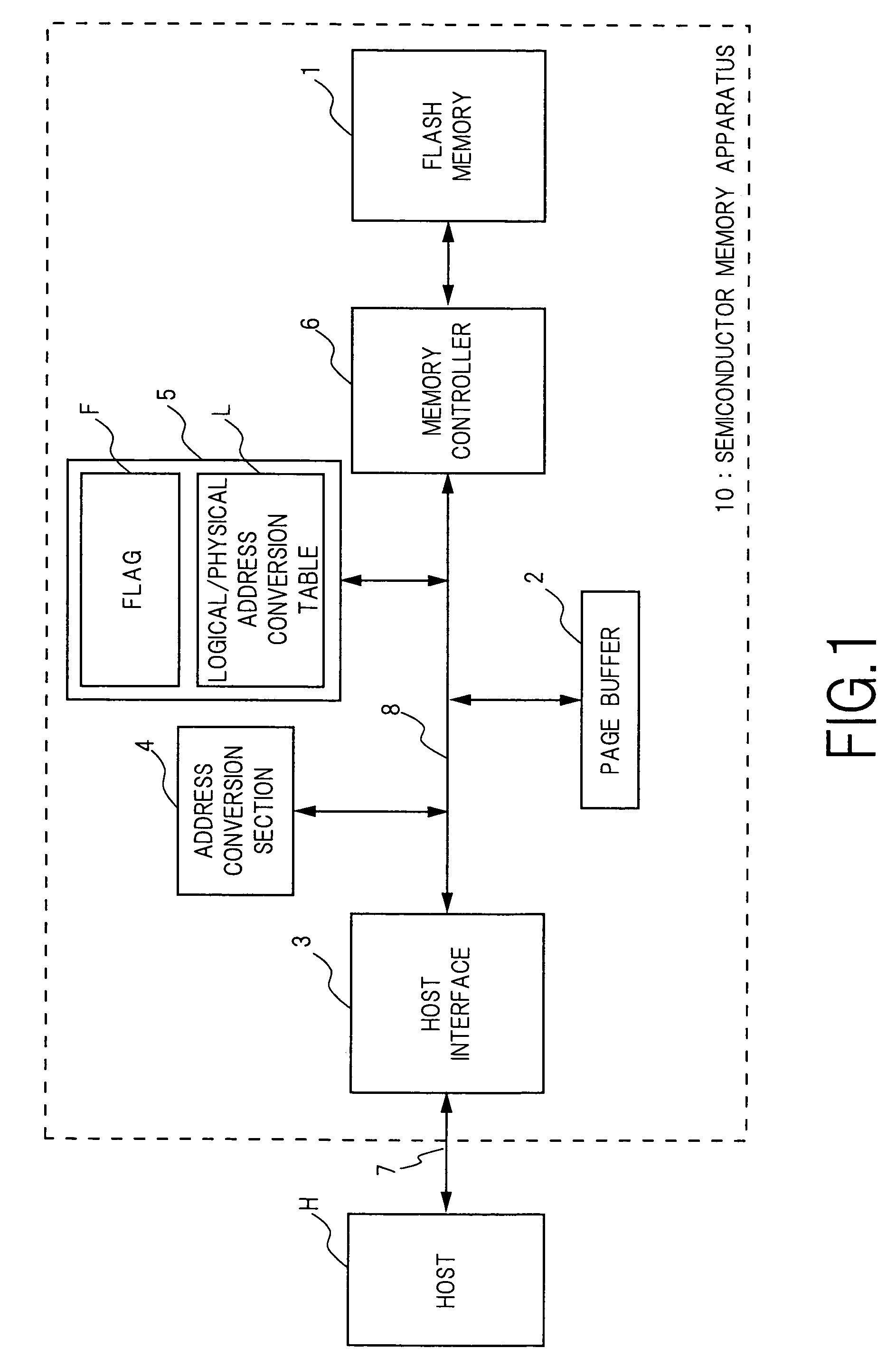
[0048]FIG. 1 is the block diagram showing the semiconductor memory apparatus 10 according to the embodiment of the present invention. The semiconductor memory apparatus 10 is connected with the host H through an external bus 7. Here, the host H is, for example, an information processing device such as a personal computer, or a mobile appliance such as a PDA and a cellular phone. The semiconductor memory apparatus 10 may be provided for the host H either internally or externally.

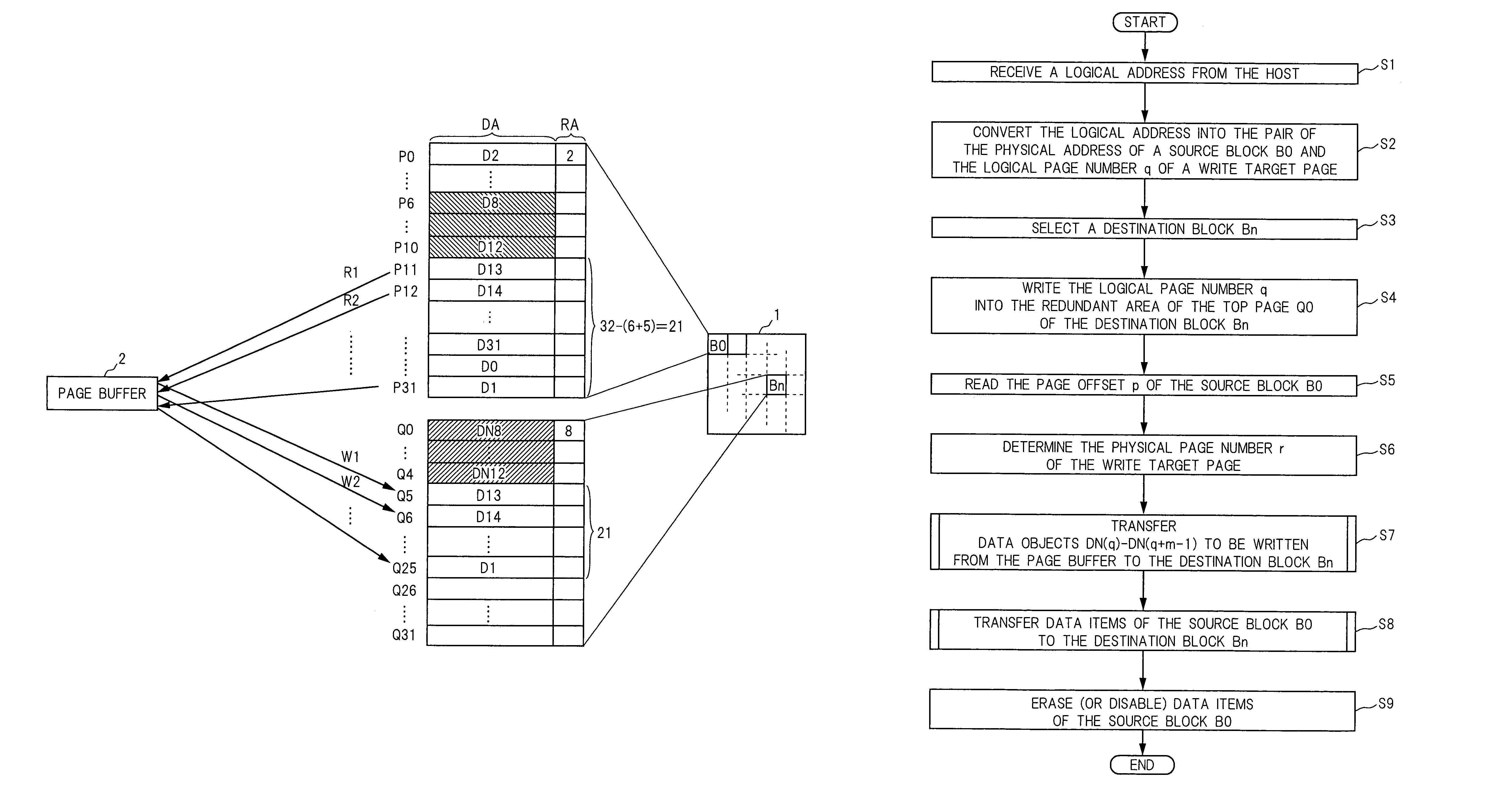
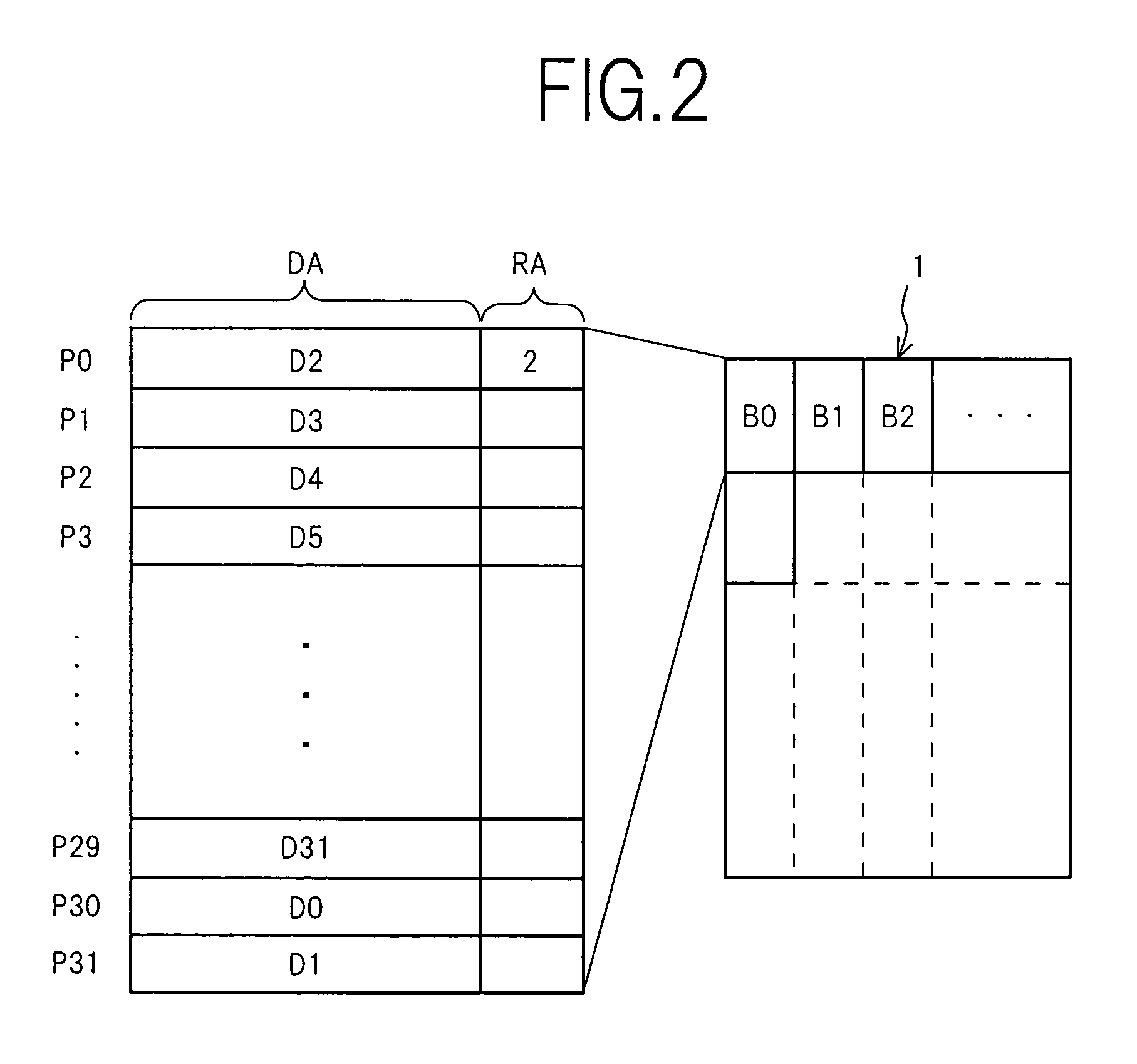
[0049]The flash memory 1 is preferably a NAND-type EEPROM (electrically erasable programmable ROM). FIG. 2 is the schematic diagram showing the outline of the structure of the cell array in the flash memory 1. The cell array is a cluster of many blocks B0, B1, B2, . . . Each block includes 32 pages, for example. The head block B0 includes 32 pages P0–P31, for example. Other blocks B1, B2, . . . , are alike. In...


PUM


Abstract

A source block (B0) and the logical page number (“8”) of a write target page are identified from the logical address of the write target page. Data objects (DN8, DN9, . . . , DN12) to be written, which a host stores in a page buffer (2), are written into the data areas (DA) of the pages (Q0, Q1, . . . , Q4) of a destination block (Bn), starting from the top page (Q0) in sequence. The logical page number (“8”) of the write target page is written into the redundant area (RA) of the top page (Q0). The physical page number (“6=8−2”) of the write target page is identified, based on the logical page number (“8”) of the write target page and the page offset (“2”) of the source block (B0). When notified by the host of the end of the sending of the data objects (DN8, . . . , DN12), the data items (D13, . . . , D31, D0, D1, . . . , D7) in the source block (B0) are transferred to the pages (Q5, Q6, . . . , Q31) in the destination block (Bn) via the page buffer (2) sequentially and cyclically, starting from the page (P11) situated cyclically behind the write target page (P6) by the number (“5”) of pages of the data objects (DN8, . . . , DN12).

Description

CROSS-REFERENCE TO RELATED APPLICATIONS[0001]This application is a section 371 of International Application No. PCT / JP03 / 10718, filed Aug. 25, 2003, the disclosure of which is incorporated herein by reference.[0002]The present invention relates to a semiconductor memory apparatus that includes a flash memory device. In particular, the invention relates to a method of writing data into the flash memory device.BACKGROUND ART[0003]Information processing appliances and, further in recent years, household electric appliances, such as television sets and refrigerators, include CPUs and realize advanced operating control by software. The appliances store (firmware) programs for the operating control and parameters in ROMs. Semiconductor memory apparatuses that include flash memory devices are extensively used as the ROMs. In addition, the semiconductor memory apparatuses are extensively used in portable information processing appliances (mobile appliances), such as notebook computers, pers...

Claims


Application Information

Patent Timeline
IPC IPC(8): G06F12/00G06F12/02G06F12/08
CPCG06F12/0246G06F2212/7203G06F12/00
Inventor INAGAKI, YOSHIHISAHONDA, TOSHIYUKI
Owner PANASONIC CORP
Why Eureka
Try Eureka