Test kit for testing a chip subassembly and a testing method by using the same

a chip sub-assembly and test kit technology, applied in electrical testing, measurement devices, instruments, etc., can solve the problem of eliminating the entire device, and achieve the effect of reducing the manufacture cost and improving the final yield of semiconductor packages

Inactive Publication Date: 2011-06-30
ADVANCED SEMICON ENG INC
View PDF4 Cites 7 Cited by
  • Summary
  • Abstract
  • Description
  • Claims
  • Application Information

AI Technical Summary

Benefits of technology

[0008]A test kit for testing a chip subassembly and a testing method by using the same is provided. The test kit and the testing method can screen out the failed device to improve the final yield of semiconductor packages and reduce the manufacture cost thereof.

Problems solved by technology

The failure may be due to the failure of one of the three dies, with the other two dies being properly functional.
Due to the increased number of dies in the package, there is an increased possibility of including a die that, while passing the wafer probe test, would actually fail in more complete test for the multi-die semiconductor package, causing the entire device to be eliminated.

Method used


Image

  • Test kit for testing a chip subassembly and a testing method by using the same
  • Test kit for testing a chip subassembly and a testing method by using the same
  • Test kit for testing a chip subassembly and a testing method by using the same

Examples


first embodiment

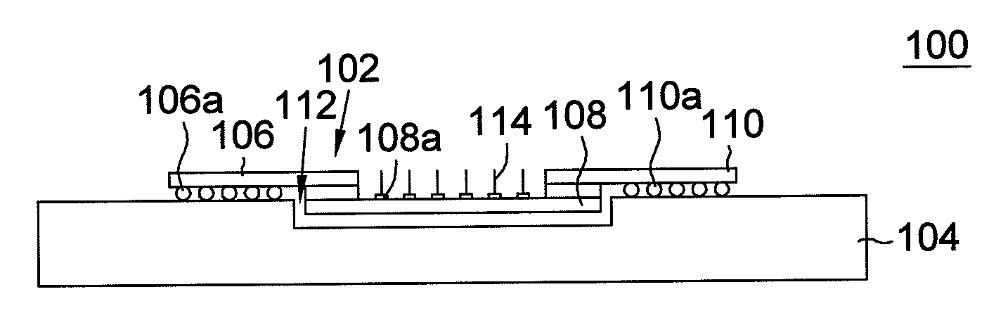
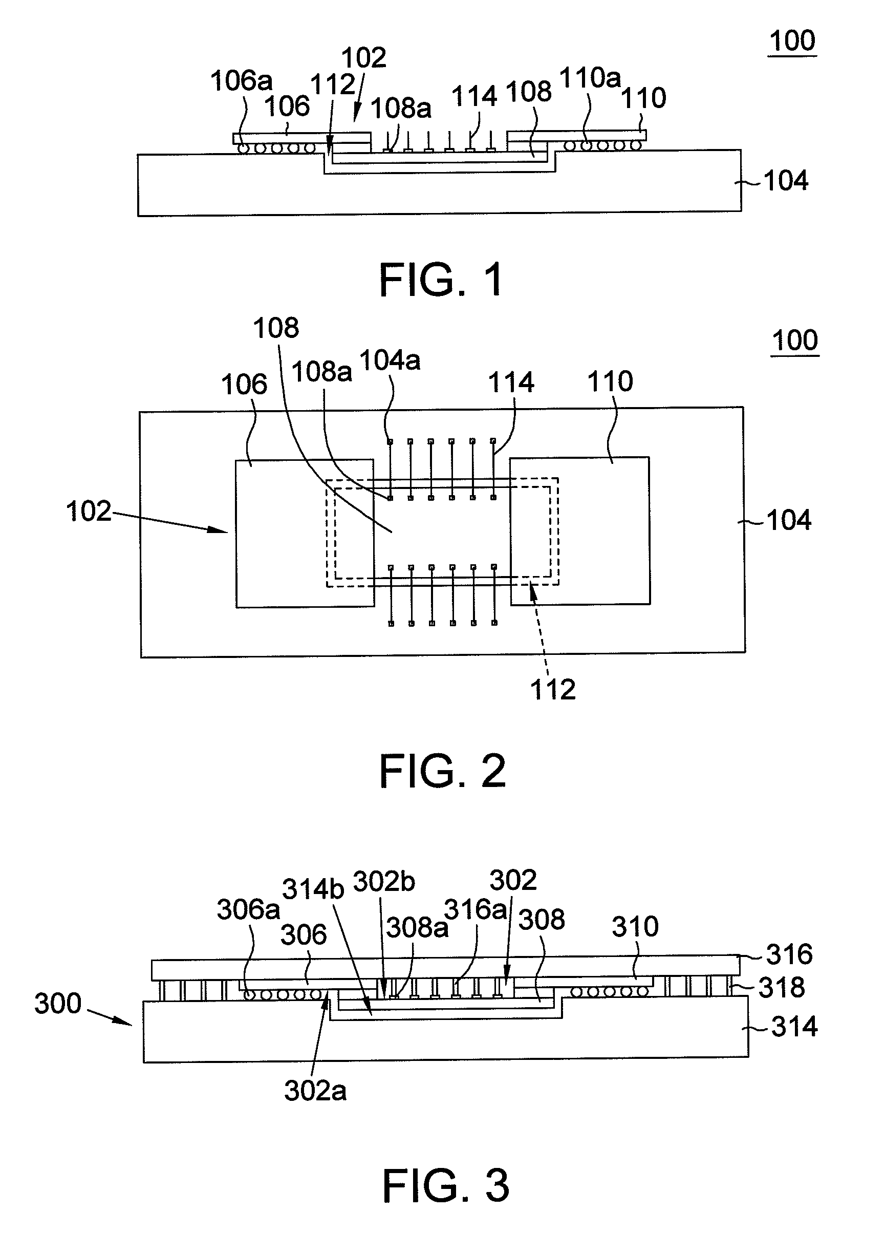
[0020]Assume the function of the semiconductor package 100 shown in FIG. 1 and FIG. 2 is to be test. FIG. 1 shows the side view of the semiconductor package 100 and FIG. 2 shows the top view of the semiconductor package 100. The semiconductor package 100 includes a chip subassembly 102 and a substrate 104. Take the chip subassembly 102 including chips 106, 108, and 110 for example. The chips 106 and 108 are in stacked relation, and the chips 108 and 110 are in stacked relation. The chip 108 is disposed between the chips 106 and 110. Each of the chips 106, 108, and 110 has electric contacts. For example, the chip 106 has a number of bumps 106a, the chip 108 has a number of wire pads 108a, and the chip 110 has a number of bumps 110a.

[0021]In the semiconductor package 100, the chip subassembly 102 is attached on the substrate 104. The substrate 104 has a cavity 112 for receiving the chip 108. The chip 106 is electrically connected to the substrate 104 through bumps 106a, the chip 108 ...

second embodiment

[0031]Referring to FIG. 5, a side view of a test kit 500 for testing the chip subassembly 502 according to a second embodiment of the disclosure is illustrated. The difference between the test kit 300 of the first embodiment and the test kit 500 of the second embodiment are described as follows.

[0032]Comparing with the test kit 300, the test kit 500 further includes a golden substrate 520 and a test substrate 522. The test substrate 522 is electrically connected to the golden substrate 520. For example, the golden substrate 520 has a number of bumps 520a for electrically connecting the test substrate 522 with the golden substrate 520. The test socket 514 further has a number of third probes 514a for electrically connecting the test socket 514 and the golden substrate 520.

[0033]The golden substrate 520 is substantially the same with the substrate 104, and the golden substrate 520 is the substrate which functions properly.

[0034]In the first embodiment, the test socket 314 simulates th...


PUM


Abstract

A test kit for testing a chip subassembly and a testing method by using the same is provided. The chip subassembly includes at least two stacked chips each having a number of electric contacts is provided. The test kit includes a test socket and a test plate. The test socket is configured to electrically engage the electric contacts on a first side of the chip subassembly. The test plate has at least a number of first probes configured for electrically engaging the electric contacts on a second side of the chip subassembly. At least one of the test socket and the test plate has a number of second probes for electrically connecting the test socket and the test plate.

Description

BACKGROUND OF THE DISCLOSURE[0001]1. Technical Field[0002]The invention relates in general to a test kit and a testing method, and more particularly to a test kit for testing a chip subassembly and a testing method by using the same.[0003]2. Description of the Related Art[0004]As is well known, with a die as part of a wafer, the die (and the other dies of the wafer) is tested by means of probes for some functions of the die.[0005]While such a wafer probe test with the die as part of a wafer is not a complete test of all functions of the die, it is helpful in eliminating the die which proves to be defective in such test. After that, the wafer is then sawed into individual dies, and each die is disposed on a substrate and then packaged as a semiconductor package. Complete functional testing is then undertaken on the die of the semiconductor package, and failed package are eliminated.[0006]As for a multi-die semiconductor package, the testing procedure is similar to that described abov...

Claims


Application Information

Patent Timeline
Patent Type & Authority Applications(United States)
IPC IPC(8): G01R31/02G01R1/06G01R31/26
CPCG01R1/0433
Inventor CHANG, HSIAO-CHUANCHENG, MING-HSIANGTSAI, TSUNG-YUEHLAI, YI-SHAOCHEN, MING-KUN
Owner ADVANCED SEMICON ENG INC
Why Eureka
Try Eureka