Method for manufacturing display device
a display device and manufacturing method technology, applied in the direction of semiconductor devices, radio frequency controlled devices, instruments, etc., can solve the problems of difficult control of the circuit, the threshold voltage of the thin film transistor cannot perform a switching function, and the shift of the negative direction of the threshold voltage of the thin film transistor in the manufacturing process, so as to achieve low power consumption and high reliability
- Summary
- Abstract
- Description
- Claims
- Application Information
AI Technical Summary
Benefits of technology
Problems solved by technology
Method used
Image

Examples
embodiment 1
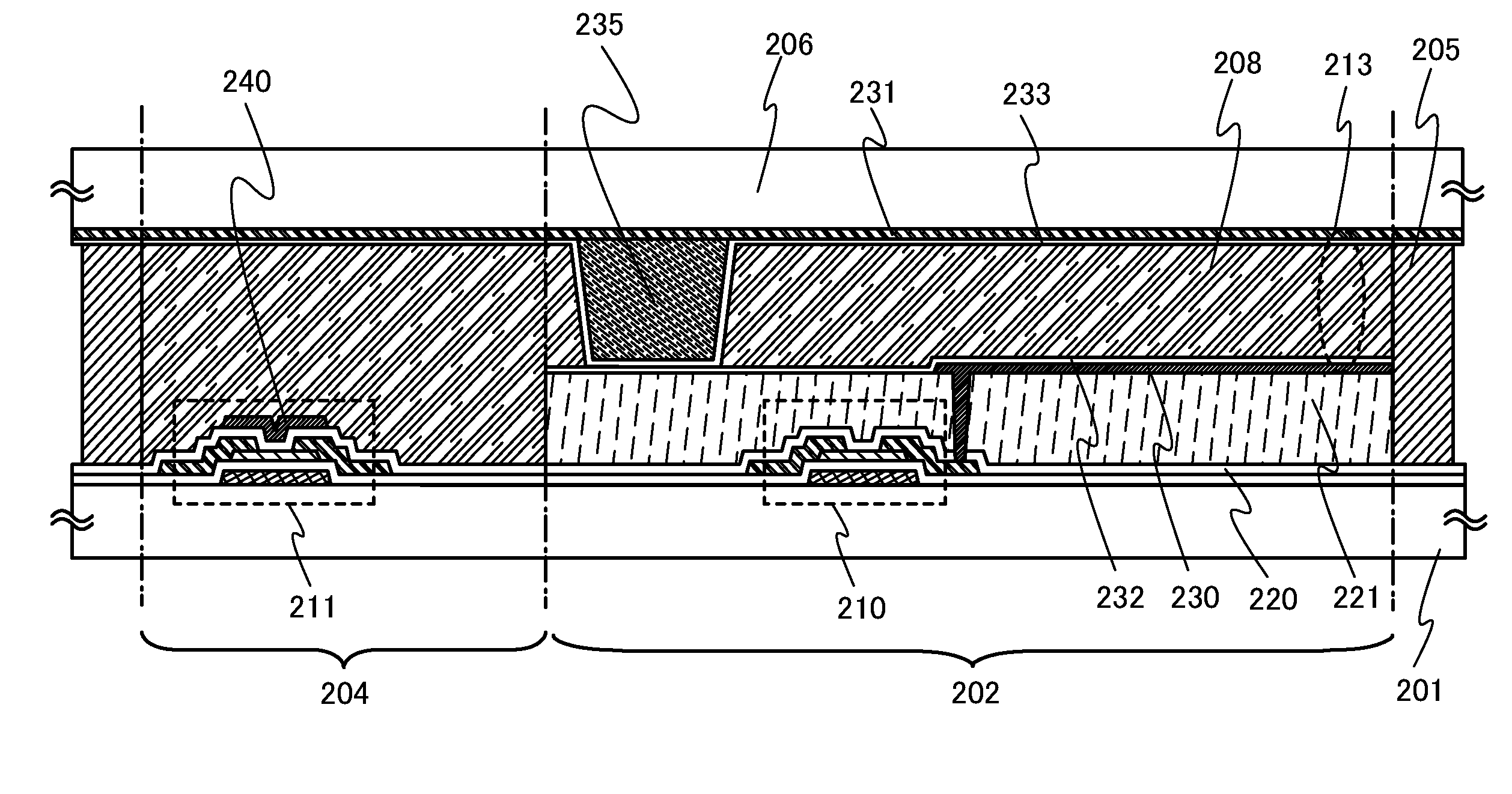
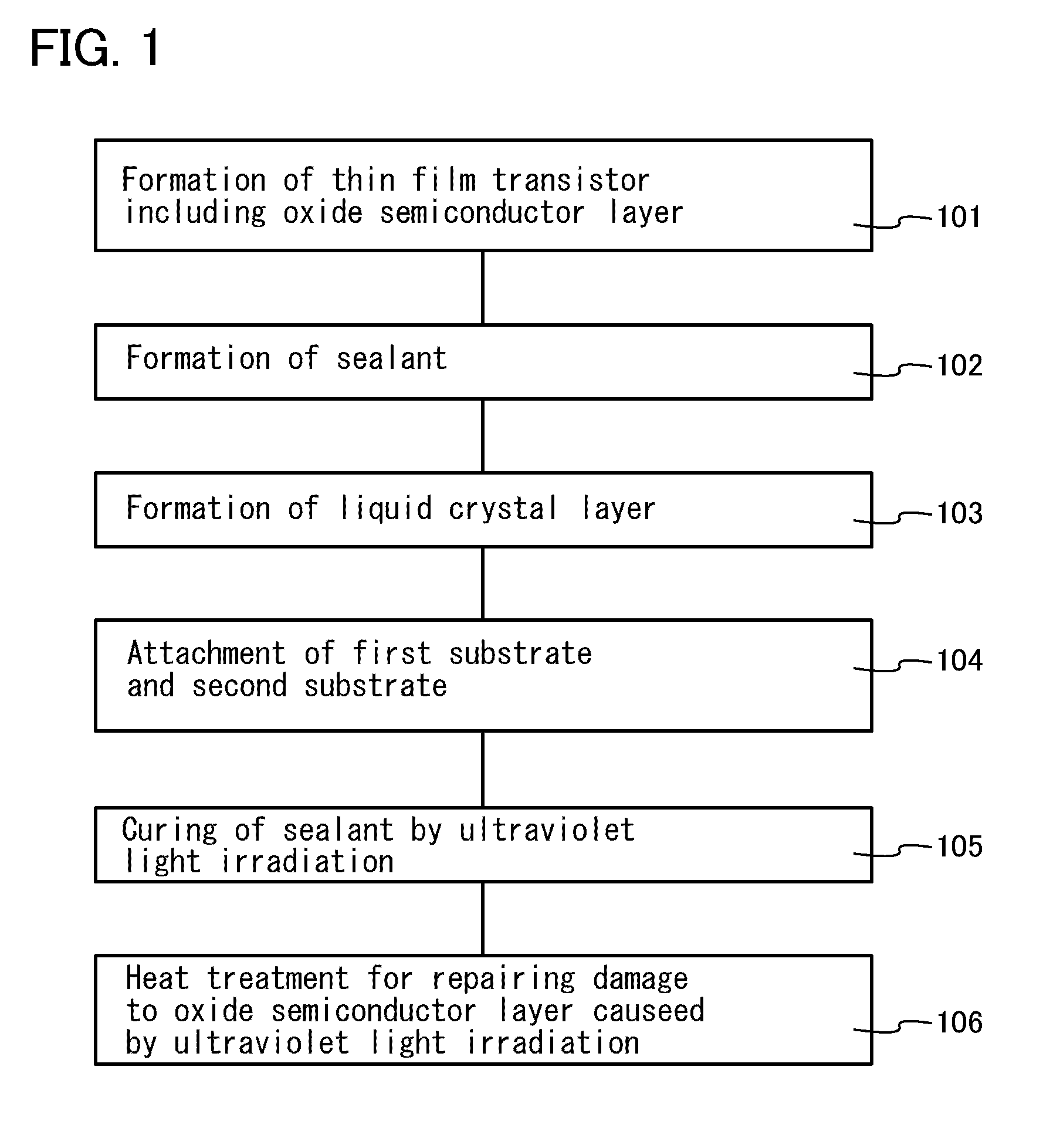
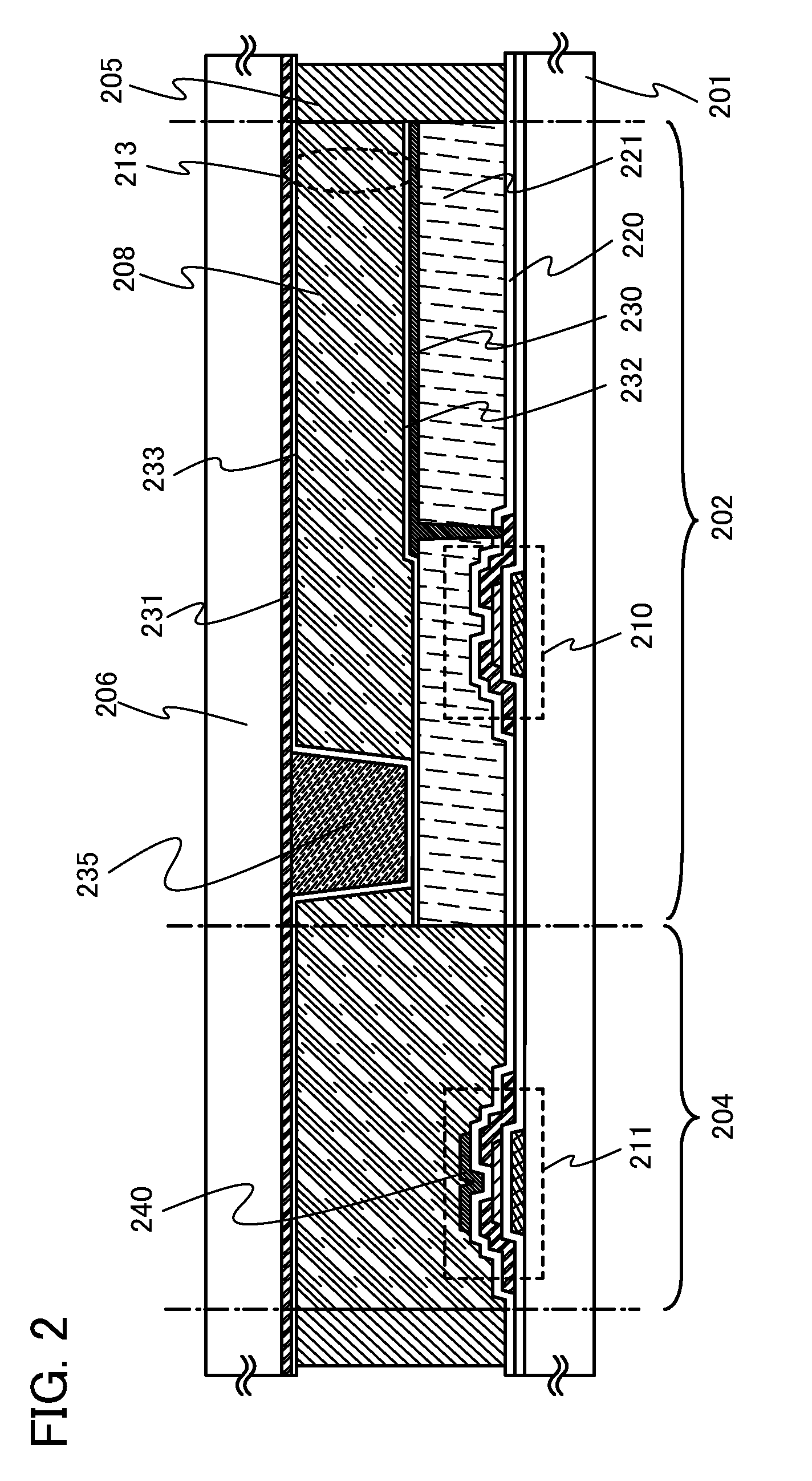
[0040]In this embodiment, a method for manufacturing a liquid crystal display device illustrated in FIG. 2, in which a thin film transistor including an oxide semiconductor layer is used, will be described with reference to a flow chart of FIG. 1. The flow chart of FIG. 1 shows steps for manufacturing the liquid crystal display device illustrated in FIG. 2 by a one drop filling method (an ODF method).
[0041]First, a structure of the liquid crystal display device illustrated in FIG. 2 will be described. In the liquid crystal display device, a liquid crystal layer 208 is sandwiched between a first substrate 201 that is an active matrix substrate and a second substrate 206 that is a counter substrate. A sealant 205 is formed between the first substrate 201 and the second substrate 206 so as to surround a pixel portion 202 and a driver circuit portion 204, and retains the distance (a cell gap) between the first substrate 201 and the second substrate 206 with a spacer 235.
[0042]The liquid...
embodiment 2
[0109]In this embodiment, a method for manufacturing a liquid crystal display device illustrated inFIG. 2, in which a thin film transistor including an oxide semiconductor layer is used, will be described with reference to a flow chart of FIG. 3. The flow chart of FIG. 3 shows steps for manufacturing the liquid crystal display device illustrated in FIG. 2 by a liquid crystal injection method.
[0110]In this embodiment, in accordance with the flow chart of FIG. 3, formation of a thin film transistor including an oxide semiconductor layer (a step 121), formation of a sealant (a step 122), attachment of a first substrate and a second substrate (a step 123), curing of the sealant by ultraviolet light irradiation (a step 124), formation of a liquid crystal layer by injection (a step 125), and heat treatment for repairing damage to the oxide semiconductor layer caused by the ultraviolet light irradiation (a step 126) will be described in this order. Note that the structure of the liquid cry...
embodiment 3
[0142]In this embodiment, a method for manufacturing a light-emitting display device illustrated in FIG. 5, in which a thin film transistor including an oxide semiconductor layer is used, will be described with reference to a flow chart of FIG. 4.
[0143]In this embodiment, as a display element included in a display device, a light-emitting element utilizing electroluminescence is used. Light-emitting elements utilizing electroluminescence are classified according to whether a light-emitting material is an organic compound or an inorganic compound. In general, the former is referred to as an organic EL element, and the latter is referred to as an inorganic EL element.
[0144]In an organic EL element, by application of voltage to a light-emitting element, electrons and holes are separately injected from a pair of electrodes into a layer containing a light-emitting organic compound, and current flows. The carriers (electrons and holes) are recombined, and thus, the light-emitting organic ...
PUM
| Property | Measurement | Unit |
|---|---|---|
| thickness | aaaaa | aaaaa |
| gate voltage | aaaaa | aaaaa |
| wavelength | aaaaa | aaaaa |
Abstract
Description
Claims
Application Information
 - R&D Engineer
- R&D Manager
- IP Professional
- Industry Leading Data Capabilities
- Powerful AI technology
- Patent DNA Extraction
Browse by: Latest US Patents, China's latest patents, Technical Efficacy Thesaurus, Application Domain, Technology Topic.
© 2024 PatSnap. All rights reserved.Legal|Privacy policy|Modern Slavery Act Transparency Statement|Sitemap