

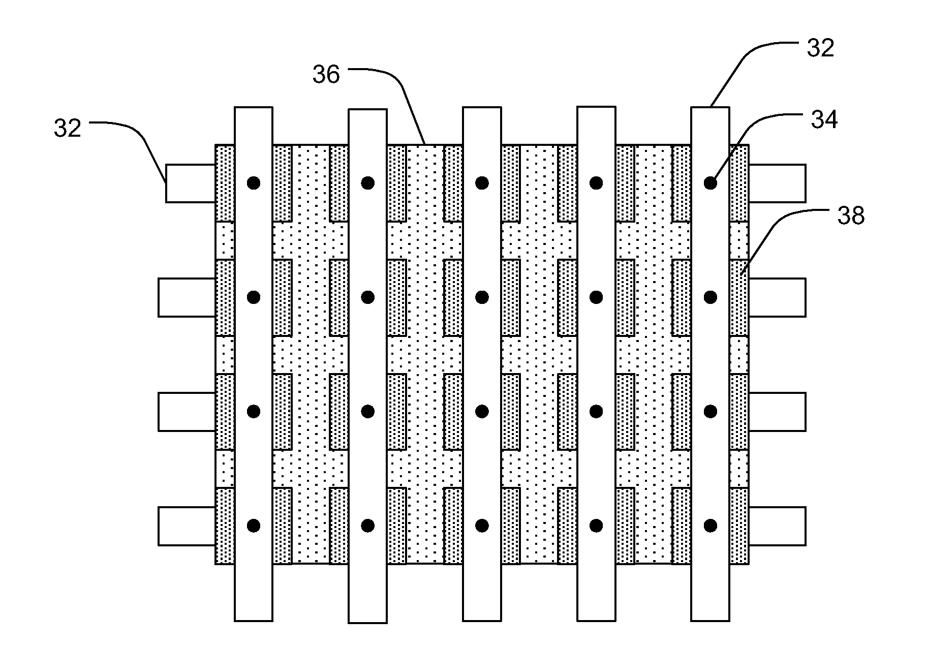
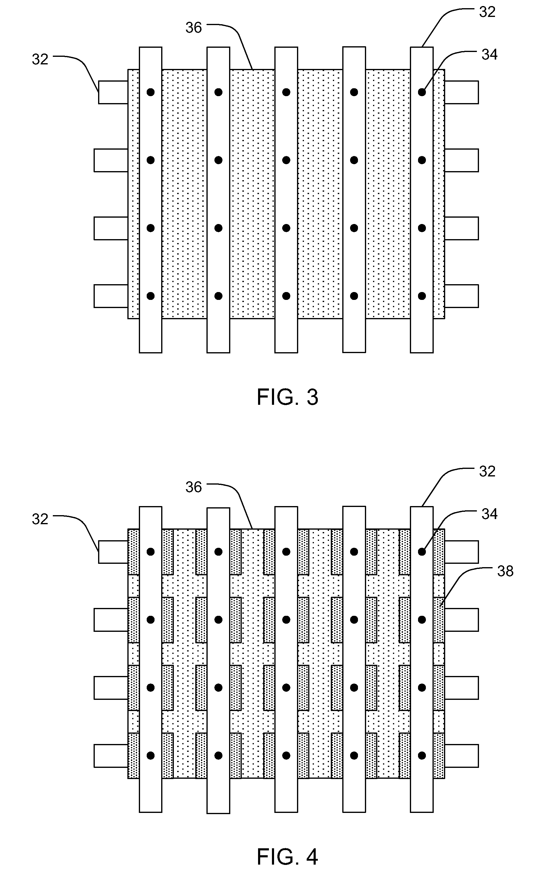
Graphene and Hexagonal Boron Nitride Devices
- Summary
- Abstract
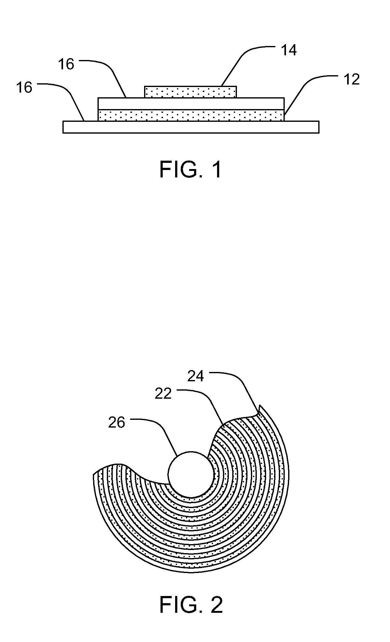
- Description
- Claims
- Application Information
AI Technical Summary
Benefits of technology
Problems solved by technology
Method used
Image

Examples
Embodiment Construction
[0015]Definitions
[0016]In describing and claiming the present invention, the following terminology will be used in accordance with the definitions set forth below.
[0017]The singular forms “a,”“an,” and, “the” include plural referents unless the context clearly dictates otherwise. Thus, for example, reference to “a layer” includes reference to one or more of such layers, and reference to “the material” includes reference to one or more of such materials.
[0018]As used herein, the term “substantially” refers to the complete or nearly complete extent or degree of an action, characteristic, property, state, structure, item, or result. For example, an object that is “substantially” enclosed would mean that the object is either completely enclosed or nearly completely enclosed. The exact allowable degree of deviation from absolute completeness may in some cases depend on the specific context. However, generally speaking the nearness of completion will be so as to have the same overall resu...
PUM
 Abstract
Description
Claims
Application Information