Method for forming conductor pattern, wiring board, and liquid droplet ejecting apapratus

Inactive Publication Date: 2011-07-14
SEIKO EPSON CORP
View PDF0 Cites 5 Cited by
  • Summary
  • Abstract
  • Description
  • Claims
  • Application Information

AI Technical Summary

Benefits of technology

According to the aspect, a liquid droplet ejecting apparatus that is favorably used for forming a conductor pa

Problems solved by technology

The photolithography method requires large-scale equipments including a vacuum apparatus and a complicated process steps, and most of the materials used is wasted due to the low material use efficiency of several percents, which increases the production cost.
However, in the case where a conductor pattern containing a pair of pad parts and a wiring part connecting the pad parts is to be formed, a conductor pattern formed by the ink-jet method may suffer cracking, breakage of wiring or the like.
The fluctuation in thickness may also depend on the pattern, for example, the difference in thickness is incr

Method used


Image

  • Method for forming conductor pattern, wiring board, and liquid droplet ejecting apapratus
  • Method for forming conductor pattern, wiring board, and liquid droplet ejecting apapratus
  • Method for forming conductor pattern, wiring board, and liquid droplet ejecting apapratus

Examples


Embodiment Construction

Preferred exemplary embodiments of the invention will be described in detail.

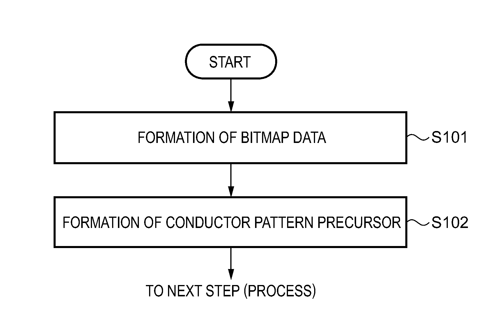
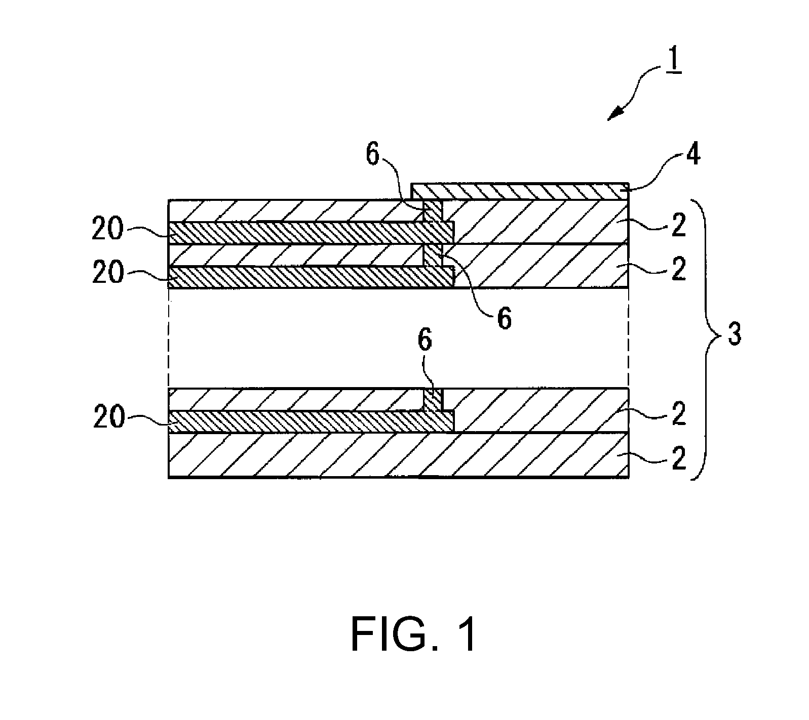
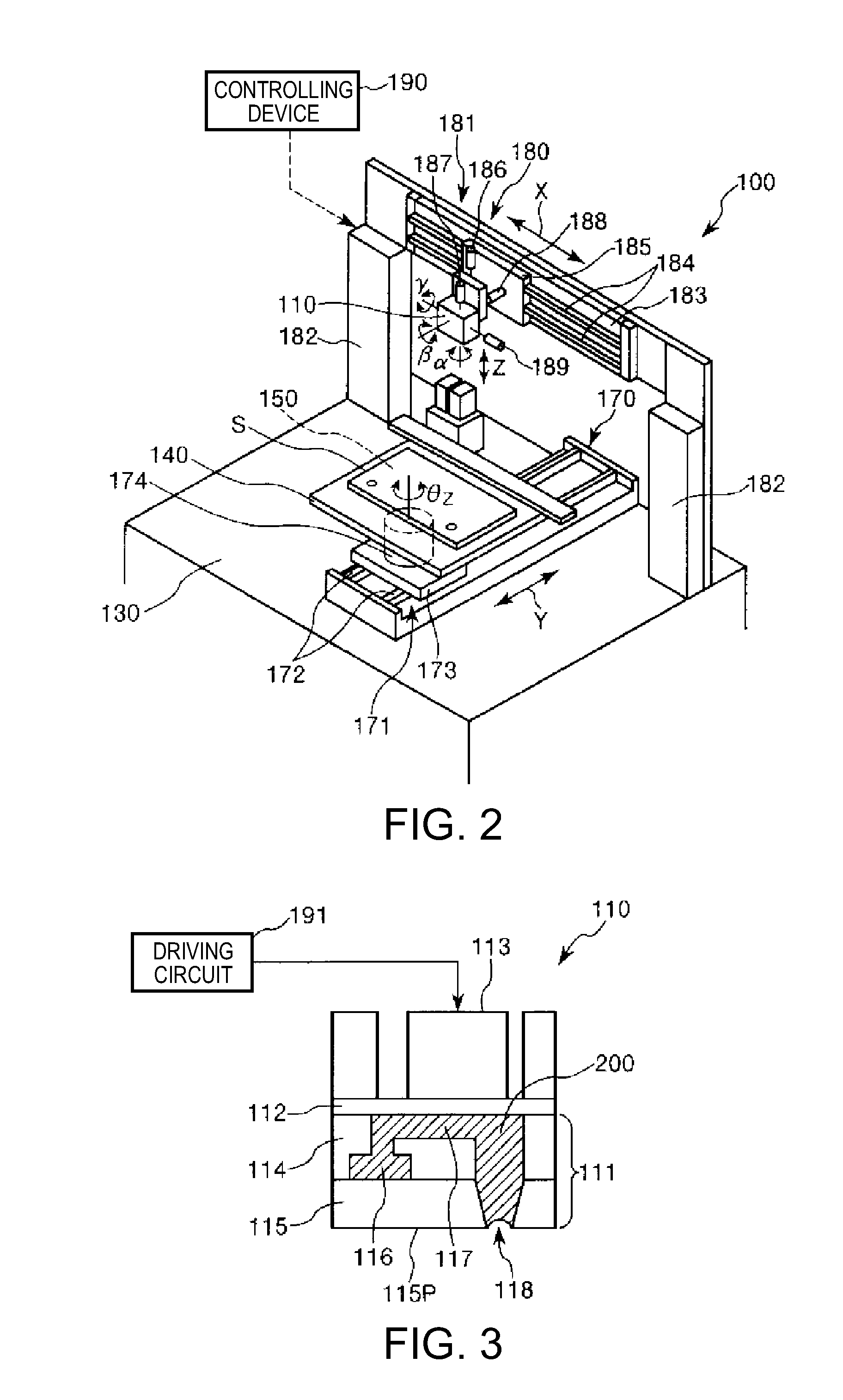
FIG. 1 is a cross sectional view showing an example of a structure of a wiring board (ceramics circuit board) according to an embodiment of the invention. FIG. 2 is a perspective view showing a schematic structure of an embodiment of an ink-jet apparatus (liquid droplet ejecting apparatus) according to an embodiment of the invention. FIG. 3 is a schematic illustration showing a schematic structure of an ink-jet head (liquid droplet ejecting head) of the ink-jet apparatus shown in FIG. 2. FIG. 4 is an illustration showing an example of a production method of the wiring board (ceramics circuit board) shown in FIG. 1. FIGS. 5A and 5B are illustrations showing an example of process steps of a production method of the wiring board (ceramics circuit board) shown in FIG. 1. FIG. 6 is a flow chart showing an embodiment of a method for forming a conductor pattern according to an embodiment of the invention (for show...


PUM


Abstract

A method for forming a conductor pattern includes: forming a conductor pattern precursor by ejecting liquid droplets of a conductor pattern forming ink by a liquid droplet ejecting method onto a substrate, and drying the liquid droplets, thereby forming a conductor pattern precursor having a pad part and a wiring part connected to the pad part on the substrate; and firing the precursor, thereby forming the conductor pattern, wherein in the formation of the conductor pattern precursor, the liquid droplets of the conductor pattern forming ink are ejected in such a manner that positions where the liquid droplets of the conductor pattern forming ink are attached form plural concentric annular shapes within a pad forming region where the pad part is to be formed on the substrate.

Description

BACKGROUND1. Technical FieldThe present invention relates to a method for forming a conductor pattern, a wiring board, and a liquid droplet ejecting apparatus.2. Related ArtWirings used in an electronic circuit and an integrated circuit are produced, for example, by a photolithography method. In the photolithography method, a photosensitive material, which is referred to as a resist, is coated on a substrate having been coated with an electroconductive film in advance and irradiated with a circuit pattern and developed, and the electroconductive film is etched according to the resist pattern, thereby forming a wiring formed of the conductor pattern. The photolithography method requires large-scale equipments including a vacuum apparatus and a complicated process steps, and most of the materials used is wasted due to the low material use efficiency of several percents, which increases the production cost.On the other hand, a liquid droplet ejecting method, in which a liquid material ...

Claims


Application Information

Patent Timeline
IPC IPC(8): B41J29/38B05C5/00B05C13/02B05D1/26B05D5/12C09D11/00C09D11/52H05K3/10
CPCH05K3/125H05K1/0306
Inventor TOYODA, NAOYUKIKOBAYASHI, TOSHIYUKIUEHARA, NOBORUHAMA, YOSHIKAZUTANABE, KENTARO
Owner SEIKO EPSON CORP
Why Eureka
Try Eureka