Adaptive Device Aging Monitoring and Compensation

a technology for adapting devices and aging monitoring, applied in the direction of measurement devices, measurement devices, instrumentation, etc., can solve the problems of significant performance loss, device aging effects become more pronounced, and the electrical parameters of semiconductor devices are degraded during normal operation

Inactive Publication Date: 2011-07-28
AVAGO TECH WIRELESS IP SINGAPORE PTE
View PDF8 Cites 37 Cited by
  • Summary
  • Abstract
  • Description
  • Claims
  • Application Information

AI Technical Summary

Problems solved by technology

Device aging (particularly in submicron geometries) results in the degradation of the electrical parameters of a semiconductor device during its normal operation.
Further, the effects of device aging become more pronounced as the device geometry gets smaller.
As a result, conventional aging c...

Method used


Image

  • Adaptive Device Aging Monitoring and Compensation
  • Adaptive Device Aging Monitoring and Compensation
  • Adaptive Device Aging Monitoring and Compensation

Examples


example aging

[0037 compensation methods according to embodiments will now be presented. These methods are presented for the purpose of illustration and not limitation.

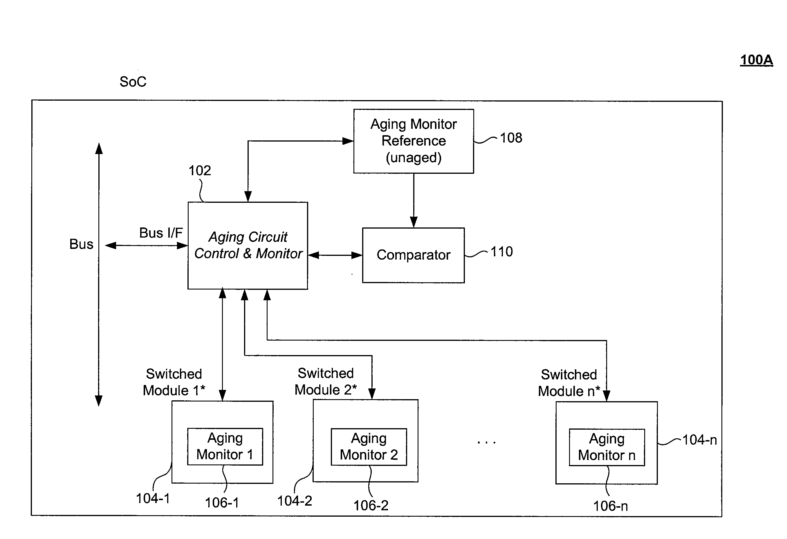
[0038]As described above, device aging in a transistor affects the threshold voltage of the transistor. This in turn affects the propagation delay through the transistor. In particular, a lower threshold voltage has the effect of lowering the propagation delay through the transistor, while a higher threshold voltage has the opposite effect and also reduces leakage current through the transistor (i.e., the current that flows through the transistor when the transistor is “OFF”).

[0039]According to an embodiment, device aging in a transistor with respect to threshold voltage can be monitored by monitoring changes in the propagation delay of the transistor. If changes from a nominal value are detected, then aging compensation is applied. In an embodiment, aging compensation is applied using a body biasing technique, further described be...


PUM


Abstract

Improved device aging monitoring and compensation schemes are presented herein. In particular, embodiments enable quantitative measurement of actual aging experienced by a device up to the instant of measurement, rather than rely on static a priori estimation of aging effects under worst case conditions. As such, embodiments provide adaptive device aging monitoring and compensation schemes. In addition, embodiments allow for aging monitoring and compensation to be performed at a desired granularity, whereby aging monitoring and compensation can be performed at a chip, module, or sub-module level. Further, embodiments inherently compensate for the effects of aging on passive components (e.g., parasitics of interconnect wires, capacitors, etc.) in addition to active device aging.

Description

BACKGROUND[0001]1. Field of the Invention[0002]The present invention relates generally to device aging monitoring and compensation.[0003]2. Background Art[0004]Device aging (particularly in submicron geometries) results in the degradation of the electrical parameters of a semiconductor device during its normal operation. Further, the effects of device aging become more pronounced as the device geometry gets smaller.[0005]Conventional aging compensation schemes estimate a priori the effects of aging on key parameters of the device. Then, based on a worst case aging scenario, device aging effects are accounted for in the design of the device by including adequate design margins such that the device meets its design requirements if the full effects of aging manifest themselves near the end of the device's operating life.[0006]As a result, conventional aging compensation schemes lead to conservative design practices and to heavily guard-banding several design parameters, which result in...

Claims


Application Information

Patent Timeline
IPC IPC(8): G01R31/26G01R31/02
CPCG01R31/3004G01R31/3016G01R31/3008
Inventor KRISHNAN, MUSARAVAKKAM
Owner AVAGO TECH WIRELESS IP SINGAPORE PTE
Why Eureka
Try Eureka