Chip-Scale Slow-Light Buffers Fashioned with Leaky-Mode Resonant Elements and Methods of Using Leaky-Mode Resonant Elements for Delaying Light

a technology of leaky-mode resonant elements and slow-light buffers, which is applied in the direction of instruments, electrical equipment, laser details, etc., can solve the problems of low reflection efficiency of pulses, inability to generate mass deployment functions, and little done to understand their dispersion properties and related slow-light applications

Inactive Publication Date: 2011-07-28
BOARD OF RGT THE UNIV OF TEXAS SYST
View PDF7 Cites 6 Cited by
  • Summary
  • Abstract
  • Description
  • Claims
  • Application Information

AI Technical Summary

Benefits of technology

[0012]A method for delaying transmitted light is presented. In some embodiments, the method may include illuminating a leaky-mode resonant element with light for a time period of no more than 1 nanosecond. The leaky-mode resonant element may be configured so that at least some of the light is transmitted in a delayed manner. In some embodiments, all of the light is transmitted in a delayed manner.

Problems solved by technology

In contrast, little has been done to understand their dispersive properties and related slow-light applications.
The technology needed to generate these functions for mass deployment is not available today, but there is a considerable amount of research being devoted to develop it.
As the spectrum of the pulse was not well accommodated by the GMR element, the reflection efficiency of the pulse was relatively low.

Method used


Image

  • Chip-Scale Slow-Light Buffers Fashioned with Leaky-Mode Resonant Elements and Methods of Using Leaky-Mode Resonant Elements for Delaying Light
  • Chip-Scale Slow-Light Buffers Fashioned with Leaky-Mode Resonant Elements and Methods of Using Leaky-Mode Resonant Elements for Delaying Light
  • Chip-Scale Slow-Light Buffers Fashioned with Leaky-Mode Resonant Elements and Methods of Using Leaky-Mode Resonant Elements for Delaying Light

Examples


example 1

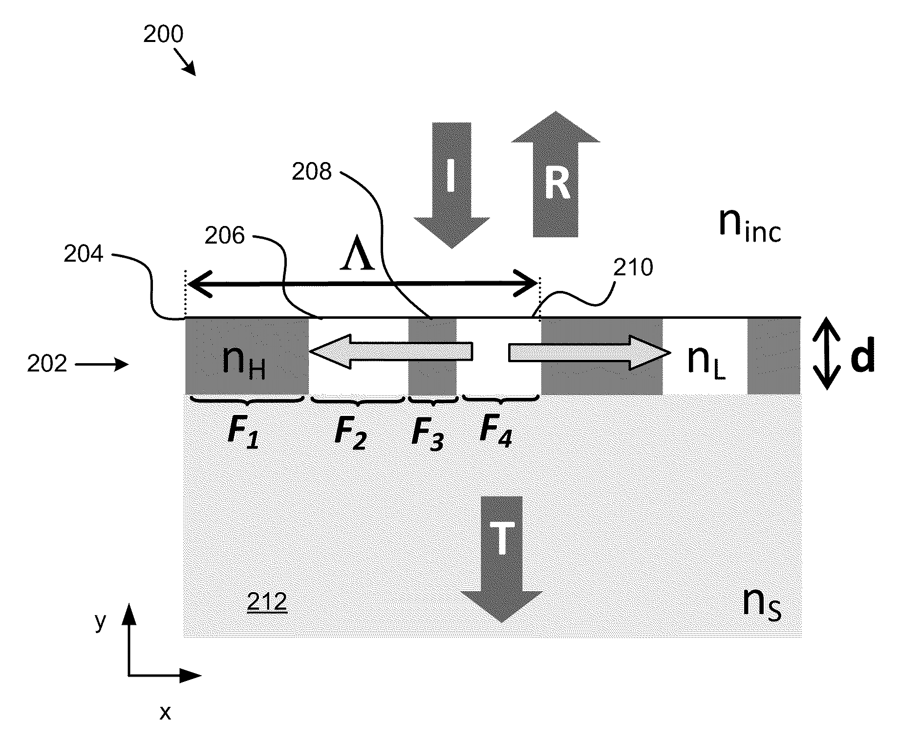
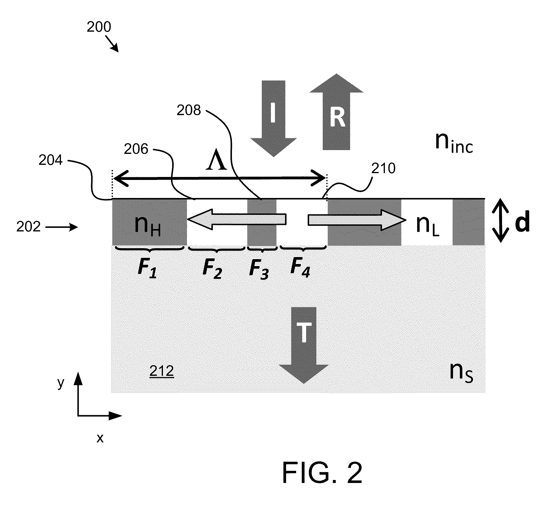
[0055]With reference to FIG. 2, an example of a silicon-on-insulator (SOI) leaky-mode resonant optical element 200 is disclosed. The spatially modulated periodic layer 202 is spatially modulated in the x-direction. It has alternating indices of refraction with a high index of refraction (nH) and a low index of refraction (nL). Components 204 and 208 have high indices of refraction, and components 206 and 210 have low indices of refraction. Components 204, 206, 208 and 210 comprise one period of the spatially modulated periodic layer. The period of spatially modulated layer 202 is denoted by Λ. Components 204, 206, 208 and 210 have widths in the x-direction of ΛF1, ΛF2, ΛF3, and ΛF4, respectively. Spatially modulated layer 202 has a depth shown by “d.” Spatially modulated periodic layer 202 is disposed on a substrate 212 having an index of refraction denoted by “nS.” The index of refraction of the medium coupled to spatially modulated layer 202 and opposite of substrate 212 is denote...

example 2

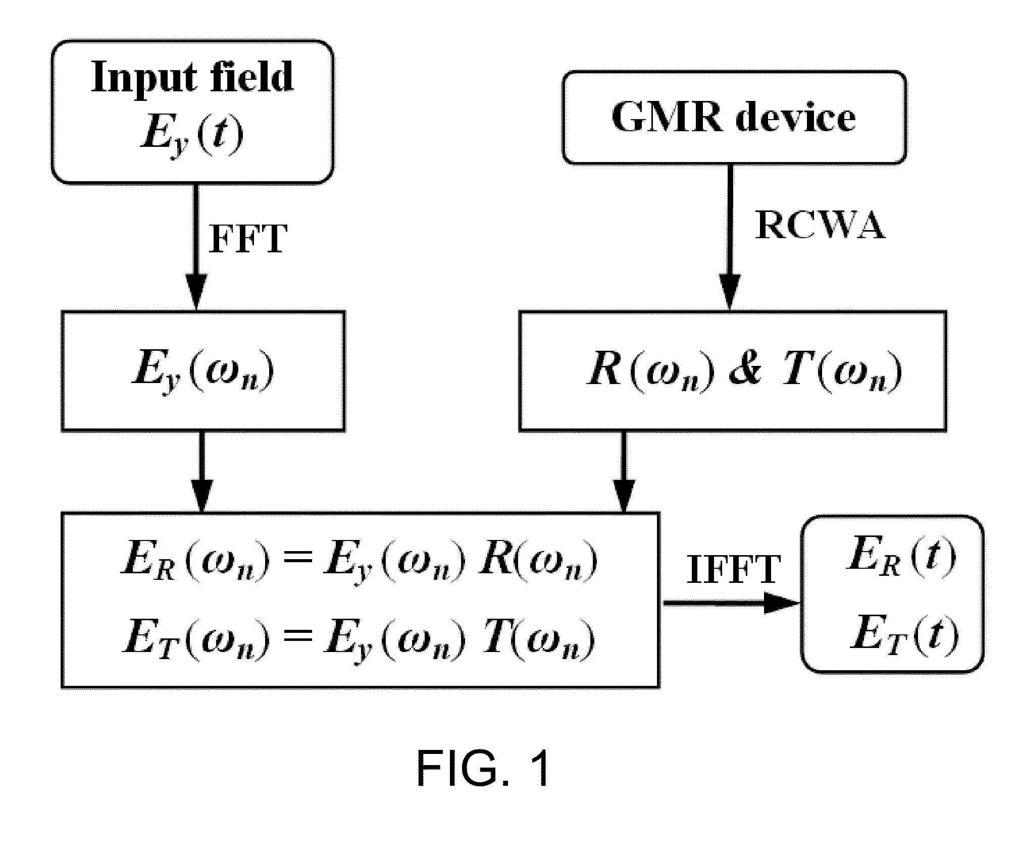
[0058]With reference to FIG. 4A, a second example is disclosed. In this example, optical element 400 includes two spatially modulated periodic layers 402 and 404, which are similar to spatially modulated periodic layer 202 shown in FIG. 2. Optical element 400 has an air gap (cavity) 406 between layers 402 and 404 to realize a ˜0.75 nm (FWHM) flat-top transmission band as shown in FIG. 4B. Again, this optical element was designed by the PSO technique described above, and its structural parameters are: Λ=1103.9 nm, d=432.2 nm, [F1, F2, F3, F4]=[0.0626, 0.3013, 0.4576, 0.1785], and dCavity=2000 nm. FIGS. 4B-E illustrate the transmittance, phase, delay, and dispersion of this device, respectively. This element shows a flat-top transmission bandwidth, which is a result of merging two adjacent narrow transmission resonances. In addition, the delay response exhibits an average of ˜7 ps in the transmission band. In comparison to the previous example, the dispersion is flatter. FIGS. 5A and ...

example 3

[0059]By cascading the structure in FIG. 4A, we can design an optical element resembling a multi-cavity photonic crystal waveguide. To illustrate, we cascaded five leaky-mode resonant subunits (NCavity=5) with spacing dB=5.0 micrometers (μm). The resulting optical element resembles the structure shown in FIG. 4A, but has ten spatially modulated periodic layers instead of two. FIGS. 6A-D show the computed results of the transmittance, phase, delay, and dispersion, respectively. Although the high-transmission bandwidth is smaller than it is for a single-layer optical element, cascading the layers results in a flat delay response of ˜30 ps over a ˜0.5 nm wavelength band. Moreover, the flat low-dispersion response illustrates that such optical elements may be used for imposing constant (and almost dispersion-free) delays on optical pulses. Theoretically, this ˜30 ps group delay for the ˜34 μm long optical element designed here corresponds to a group velocity of ˜0.0038 c (where “c” is t...


PUM


Abstract

A method for delaying transmitted light. The method may include illuminating a leaky-mode resonant element with light pulses of short duration and sequences of such pulses. The leaky-mode resonant element may include a spatially modulated periodic layer and may be configured so that at least some of the light is transmitted in a delayed manner.

Description

CROSS REFERENCE TO RELATED APPLICATION[0001]This application claims priority to U.S. Provisional Patent Application No. 61 / 286,062, filed Dec. 14, 2009, which is incorporated reference in its entirety.STATEMENT REGARDING FEDERALLY SPONSORED RESEARCH[0002]This invention was made with government support under grant number ECCS-0925774 awarded by the National Science Foundation. The government has certain rights in the invention.BACKGROUND[0003]1. Field[0004]This invention relates to methods of delaying light using leaky-mode resonant elements. The methods and devices disclosed can be applied, for example, in dispersion management and engineering in telecommunication systems, in laser systems, in optical logic devices, and in nanoelectronic and nanophotonic chips.[0005]2. Description of the Related Art[0006]Materials that are artificially structured on a nanoscale exhibit electronic and photonic properties that differ dramatically from those of the corresponding bulk entity. In particu...

Claims


Application Information

Patent Timeline
Patent Type & Authority Applications(United States)
IPC IPC(8): H01S3/105
CPCG02B6/1225G02B5/1809
Inventor MAGNUSSON, ROBERTSHOKOOH-SAREMI, MEHRDAD
Owner BOARD OF RGT THE UNIV OF TEXAS SYST
Why Eureka
Try Eureka