Atomic layer etching apparatus and etching method using the same

a technology of atomic layer and etching method, which is applied in the direction of electrical apparatus, electrical discharge tubes, decorative arts, etc., can solve the problems of physical and electrical damage to the semiconductor substrate or the specific material layer, reduced design rules, and reduced productivity

Inactive Publication Date: 2011-08-11
RES & BUSINESS FOUND SUNGKYUNKWAN UNIV
View PDF4 Cites 387 Cited by
  • Summary
  • Abstract
  • Description
  • Claims
  • Application Information

AI Technical Summary

Benefits of technology

[0016]In yet other example embodiments, in irradiating the neutral beams and removing the surface material of the layer to be etched and the radicals, the voltages applied ...

Problems solved by technology

However, since a large amount of ions for performing an etching process exist in such etching equipment and the ions collide with a semiconductor substrate or a specific material layer on the semiconductor substrate with hundreds eV of energy, physical and electrical damage to the semiconductor substrate or the specific material layer may occur.
Therefore, s...

Method used


Image

  • Atomic layer etching apparatus and etching method using the same
  • Atomic layer etching apparatus and etching method using the same
  • Atomic layer etching apparatus and etching method using the same

Examples


Embodiment Construction

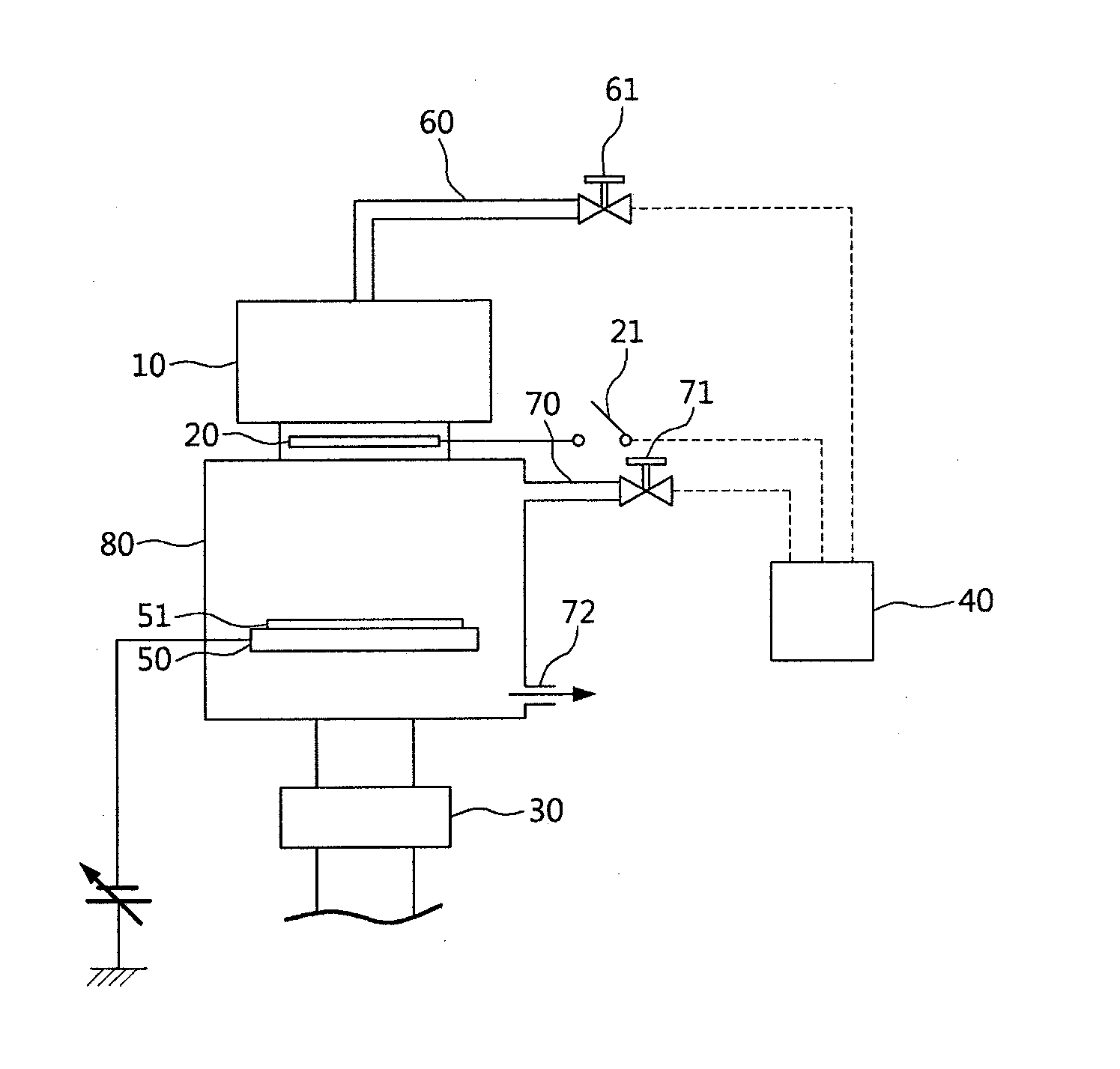
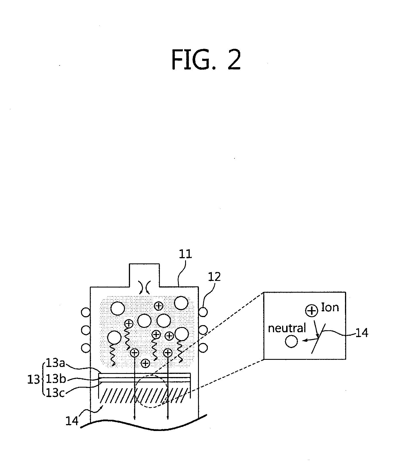
[0023]Example embodiments of the present invention are disclosed herein. However, specific structural and functional details disclosed herein are merely representative for purposes of describing example embodiments of the present invention, however, example embodiments of the present invention may be embodied in many alternate forms and should not be construed as limited to example embodiments of the present invention set forth herein.

[0024]Accordingly, while the invention is susceptible to various modifications and alternative forms, specific embodiments thereof are shown by way of example in the drawings and will herein be described in detail. It should be understood, however, that there is no intent to limit the invention to the particular forms disclosed, but on the contrary, the invention is to cover all modifications, equivalents, and alternatives falling within the spirit and scope of the invention.

[0025]It will be understood that, although the terms first, second, etc. may b...


PUM

PropertyMeasurementUnit
Poweraaaaaaaaaa
Electric potential / voltageaaaaaaaaaa
Energyaaaaaaaaaa

Abstract

An atomic layer etching apparatus using reactive radicals and neutral beams and an etching method using the same are provided. The atomic layer etching apparatus includes a reaction chamber including a stage on which a substrate to be etched is seated, a plasma generator including a plasma chamber configured to supply reactive radicals and neutral beams into the reaction chamber and receive a source gas to generate plasma, an inductive coil configured to surround the exterior of the plasma chamber to generate an electric field, a grid assembly disposed at a lower part of the plasma chamber and including first, second and third grids for extracting ion beams, and a reflective body disposed under the grid assembly and configured to supply electrons to the ion beams to convert the ion beams into neutral beams, a shutter installed between the plasma generator and the reactive chamber and configured to adjust supply of the neutral beams into the reaction chamber, a purge gas supply part configured to supply a purge gas into the reaction chamber, and a controller configured to control supply of the source gas, an etching gas and the purge gas, and opening/closing of the shutter.

Description

CLAIM FOR PRIORITY[0001]This application claims priority to Korean Patent Application No. 2010-11929 filed on Feb. 9, 2010 in the Korean Intellectual Property Office (KIPO), the entire contents of which are hereby incorporated by reference.BACKGROUND[0002]1. Technical Field[0003]Example embodiments of the present invention relate in general to the field of an atomic layer etching apparatus and an etching method using the same, and more specifically, to an atomic layer etching apparatus using reactive radicals and neutral beams, and an etching method using the same.[0004]2. Related Art[0005]As high integration of semiconductor devices has been continuously needed, in recent times, design rules for semiconductor integration circuits have been further reduced so that critical dimensions of 0.25 μm or less are required. Now, as etching equipment for implementing a nanometer-sized semiconductor device, ion-enhanced etching equipment such as a high density plasma etcher, a reactive ion et...

Claims


Application Information

Patent Timeline
IPC IPC(8): B44C1/22H01L21/3065
CPCH01J37/32009H01J37/32357H01L21/32137H01L21/3065H01J37/32422
Inventor YEOM, GEUN-YOUNGLIM, WOONG-SUNPARK, SANG-DUKKIM, YI-YEONPARK, BYOUNG-JAEYEON, JE-KWAN
Owner RES & BUSINESS FOUND SUNGKYUNKWAN UNIV
Why Eureka
Try Eureka