Semiconductor device and semiconductor module

a semiconductor module and semiconductor technology, applied in semiconductor devices, digital storage, instruments, etc., can solve the problems of increasing the load on the transmission line, the inability to design the asic and the dram, and the increase of the reflected wave (noise) generated by the contact with the transmission line in the dram

Inactive Publication Date: 2011-08-11
LONGITUDE LICENSING LTD
View PDF4 Cites 5 Cited by
  • Summary
  • Abstract
  • Description
  • Claims
  • Application Information

AI Technical Summary

Benefits of technology

[0038]Consequently, there is an effect in which, in both the upper and lower semiconductor devices, the signal paths between the semiconductor devices and the substrate can be set to substantially equal lengths for a data signal and a strobe signal.

Problems solved by technology

However, when the number of DRAMs connected to a transmission line of the ASIC increases, reflected waves (noise) generated from contacts with the transmission line in the DRAMs increase and the load on the transmission line also increases.
This makes it difficult to design the ASIC and the DRAMs.
The DQ signal particularly tends to be affected by noise.
Since the DQS signal operates at the same speed in association with the DQ signal, the DQS signal also tends to be affected by noise like the DQ signal.
In this case, as regards the DRAMs, it is costly to separately manufacture the ×8 operation chips and the ×16 operation chips.

Method used


Image

  • Semiconductor device and semiconductor module
  • Semiconductor device and semiconductor module
  • Semiconductor device and semiconductor module

Examples


Embodiment Construction

[0046]The invention will be now described herein with reference to illustrative embodiments. Those skilled in the art will recognize that many alternative embodiments can be accomplished using the teachings of the present invention and that the invention is not limited to the embodiments illustrated for explanatory purposes.

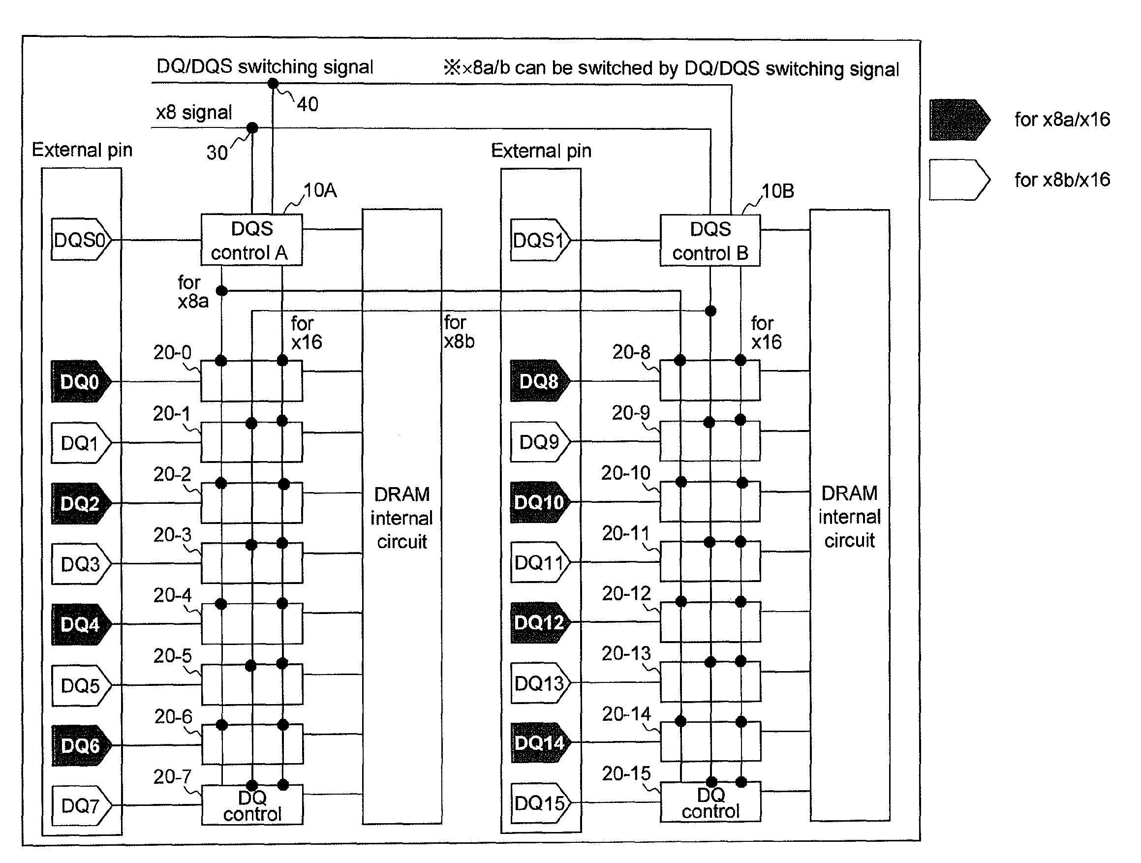
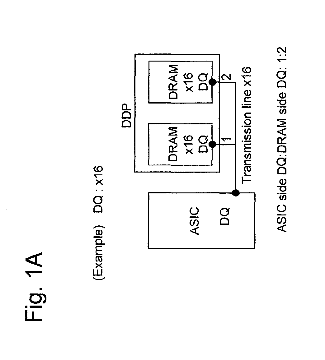
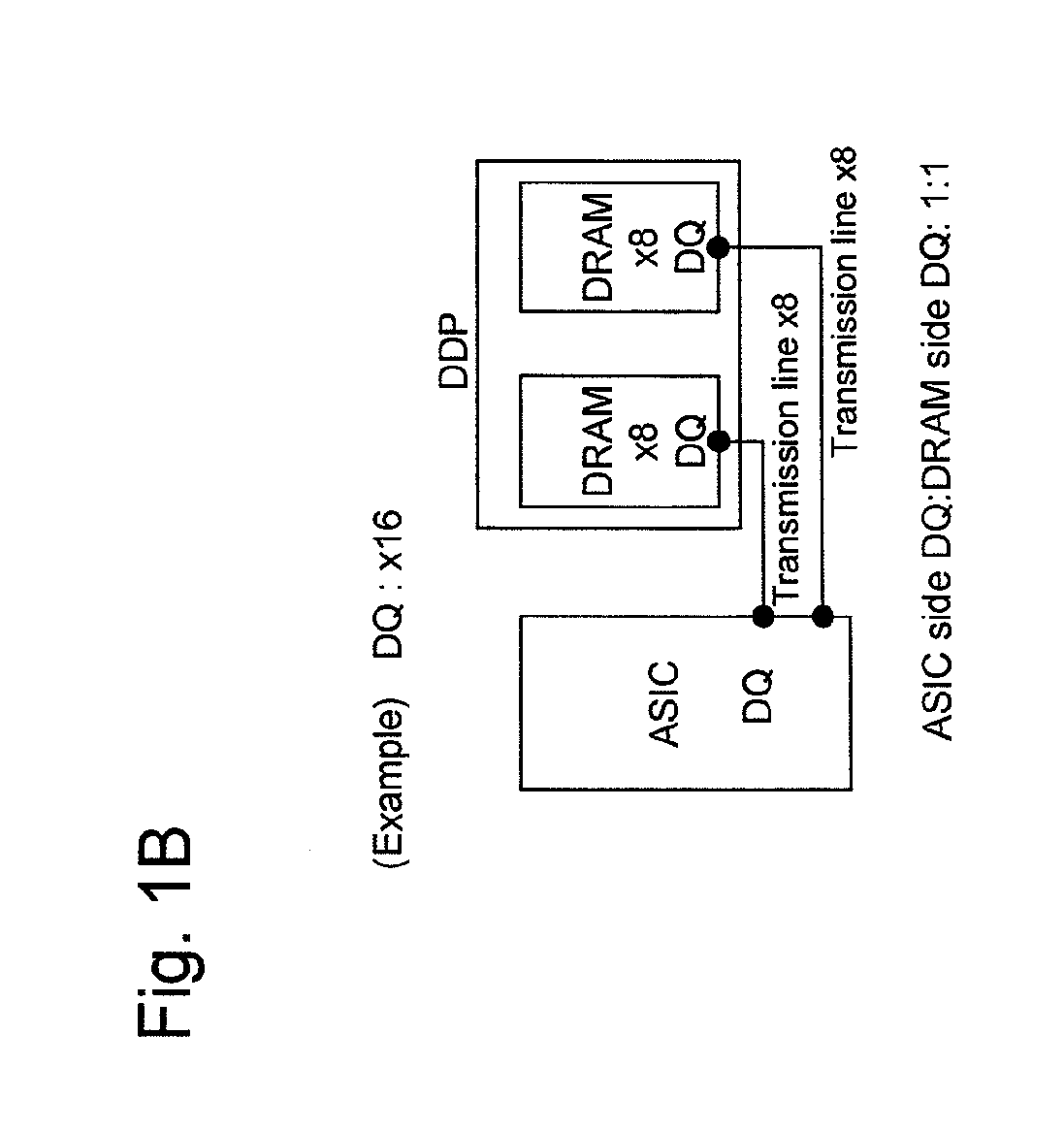
[0047]A semiconductor module according to an exemplary embodiment of the present invention is explained as having a DDP structure in which two DRAM chips as semiconductor devices, are stacked on a PKG substrate, including sixteen DQ pins for each of the DRAMs, and which is capable of switching ×8 operation and ×16 operation.

[0048]Each of the upper and lower DRAMs mounted on the semiconductor module according to this exemplary embodiment includes, as shown in FIG. 3, DQS control circuit 10A provided to correspond to a DQS0 pin on the PKG substrate, DQS control circuit 10B provided to correspond to a DQS1 pin on the PKG substrate, DQ control circuits 20-0˜20-15 pro...


PUM


Abstract

A semiconductor device according to the present invention performs, when a first word structure is designated, control such that input and output of data is performed from a first data input/output terminal and from a second data input/output terminal in response to a first strobe signal and a second strobe signal. The semiconductor device performs, when a second word structure is designated and when a first control signal is supplied, control such that input and output of data is performed from the first data input/output terminal in response to the first strobe signal. The semiconductor device performs, when the second word structure is designated and when a second control signal is supplied, control such that input and output of data is performed from the second data input/output terminal in response to the second strobe signal.

Description

BACKGROUND OF THE INVENTION[0001]1. Field of the Invention[0002]The present invention relates to a semiconductor device and a semiconductor module mounted with the semiconductor device.[0003]2. Description of Related Art[0004]In recent years, ASIC (Application Specific Integrated Circuit) and DRAM (Dynamic Random Access Memory) are used on the inside of digital home electronic appliances in order to perform various information processing and control operations.[0005]The ASIC and the DRAM are mainly connected in a one-to-one ratio. However, according to diversification of information processing and complication of control, there is a demand for an increase in the memory capacity of the DRAM in the same package (PKG). Therefore, in recent years, as shown in FIG. 1A, ASIC and DRAMs are connected in a one-to-two ratio. The ASIC is actuated to selectively control the DRAMs using a chip selection signal.[0006]However, when the number of DRAMs connected to a transmission line of the ASIC i...

Claims


Application Information

Patent Timeline
Patent Type & Authority Applications(United States)
IPC IPC(8): G11C7/10G11C7/00
CPCG11C5/04G11C8/18G11C11/4093G11C11/4076G11C7/02H01L2224/48091H01L2224/48145H01L2924/00014H01L2924/00012
Inventor NARA, MASARU
Owner LONGITUDE LICENSING LTD
Why Eureka
Try Eureka