Memory system

a memory system and memory technology, applied in the field of memory systems, can solve problems such as adversely affecting writing/erasing characteristics closely related to a li

Active Publication Date: 2011-08-11
KIOXIA CORP
View PDF5 Cites 33 Cited by
  • Summary
  • Abstract
  • Description
  • Claims
  • Application Information

AI Technical Summary

Problems solved by technology

It is known that when the writing / erasing is performed many times, a gate oxide film around the floating gate is degraded, which adversely affects writing / erasing characteristics closely related to a life of the NAND-type flash memory.

Method used


Image

  • Memory system
  • Memory system
  • Memory system

Examples


first embodiment

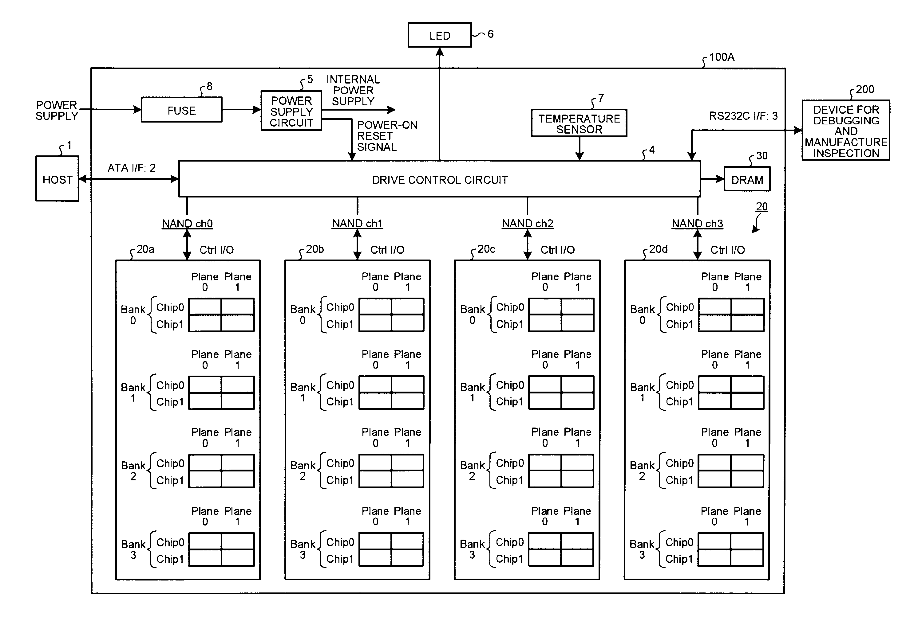
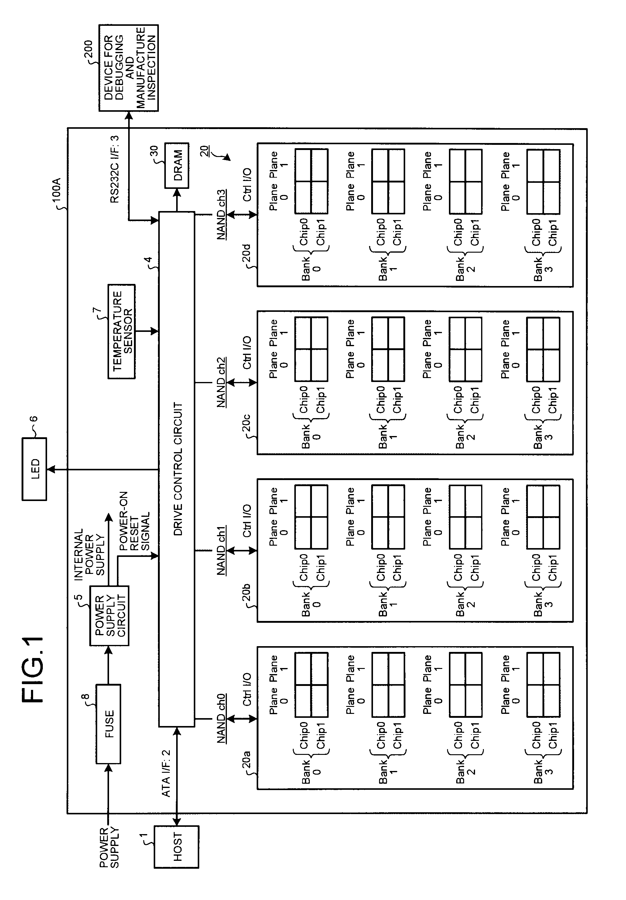
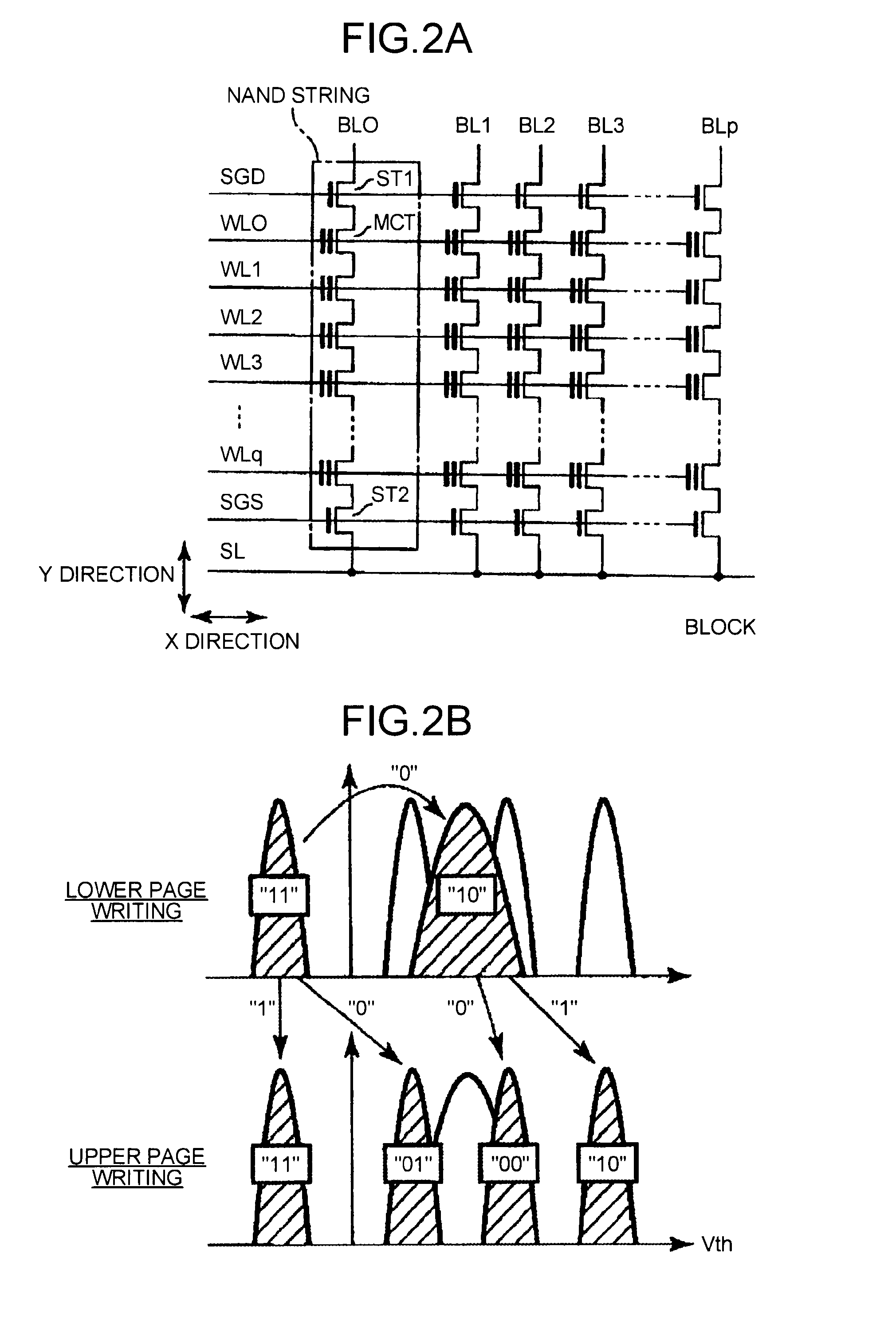
In the present embodiment, a loop count of an applied voltage in writing or erasing to a memory cell of a NAND-type flash memory is detected for determining a life (degraded state) of an SSD (Solid State Drive) that includes the NAND-type flash memory as one example of a nonvolatile semiconductor memory. The loop count in this example is the number of pulses (number of voltage applications) of a voltage applied to the NAND-type flash memory in writing or erasing to the NAND-type flash memory. In writing or erasing, a predetermined voltage is applied to the NAND-type flash memory a plurality of times (for the loop count) while gradually increasing the voltage.

After detecting the loop count of the applied voltage, the loop count is compared with a preset setting value (predetermined threshold), and the degraded state of each block in the NAND-type flash memory is determined based on this comparison result. Moreover, the degraded state of the SSD (whole memory system including a plural...

second embodiment

Next, the memory system according to the second embodiment is explained. In the second embodiment, the loop count management table 31 is sent from the SSD (SSD 100B to be described later) to the host 1 that is an external device and the host 1 performs the life determination of the SSD 100B.

FIG. 14 is a functional block diagram illustrating a functional configuration example of the SSD according to the second embodiment of the present invention. Components that achieve the same function as the SSD 100A shown in FIG. 5 among components in FIG. 14 are given the same reference numerals and overlapping explanation is omitted. The host 1 in the present embodiment includes a life managing unit 16. The life managing unit 16 has a function similar to the life managing unit 14 included in the SSD 100A explained in the first embodiment.

The SSD 100B as the memory system shown in FIG. 14 includes a controller 10B, the NAND memory 20, the DRAM 30, and the host I / F 40. The controller 10B has a fu...


PUM


Abstract

According to the embodiments, a memory system includes a nonvolatile semiconductor memory and a writing-loop-count monitoring unit that monitors a loop count of an applied voltage to the nonvolatile semiconductor memory required for data writing of the nonvolatile semiconductor memory as a writing loop count. Moreover, the memory system includes a management table for managing the writing loop count in block unit that is a unit of data erasing and a life managing unit that determines a degraded state of the nonvolatile semiconductor memory based on the management table.

Description

CROSS-REFERENCE TO RELATED APPLICATIONSThis application is based upon and claims the benefit of priority from the prior Japanese Patent Application No. 2010-27944, filed on Feb. 10, 2010; the entire contents of which are incorporated herein by reference.FIELDThe present embodiments typically relate to a memory system.BACKGROUNDA NAND-type flash memory is a semiconductor memory that needs erase processing before performing writing. In writing / erasing of data in the NAND-type flash memory, electrons are injected / removed in / from a floating gate by applying a high voltage between a substrate and a control gate. It is known that when the writing / erasing is performed many times, a gate oxide film around the floating gate is degraded, which adversely affects writing / erasing characteristics closely related to a life of the NAND-type flash memory. Therefore, it is desired to correctly recognize the life of the NAND-type flash memory.BRIEF DESCRIPTION OF THE DRAWINGSFIG. 1 is a configuration ...

Claims


Application Information

Patent Timeline
Patent Type & Authority Applications(United States)
IPC IPC(8): G06F12/06
CPCG06F12/0246G06F2212/7207G06F2212/7211G11C16/14G11C16/349G11C16/16G11C16/3445G06F11/1072G06F11/1084G06F11/3034G11C29/50004G11C2029/5004G06F3/0605G06F3/0619G06F3/064G06F3/0653G06F3/0659G06F3/0679G06F11/3058G06F11/327G06F2212/1032G06F2212/152G06F2212/214G06F2212/7201G11C29/52
Inventor OKAMOTO, SHINKEN
Owner KIOXIA CORP
Why Eureka
Try Eureka