
Stalling synchronisation circuits in response to a late data signal

a synchronisation circuit and data signal technology, applied in the field of data processing, can solve problems such as being near impossible in a large system

Active Publication Date: 2011-08-18
RGT UNIV OF MICHIGAN
View PDF6 Cites 8 Cited by
  • Summary
  • Abstract
  • Description
  • Claims
  • Application Information

AI Technical Summary

Benefits of technology

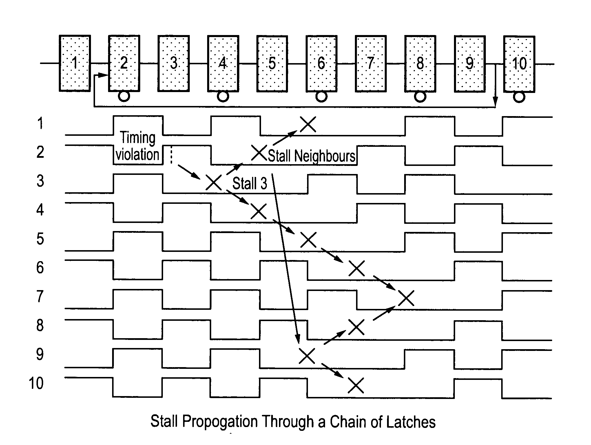
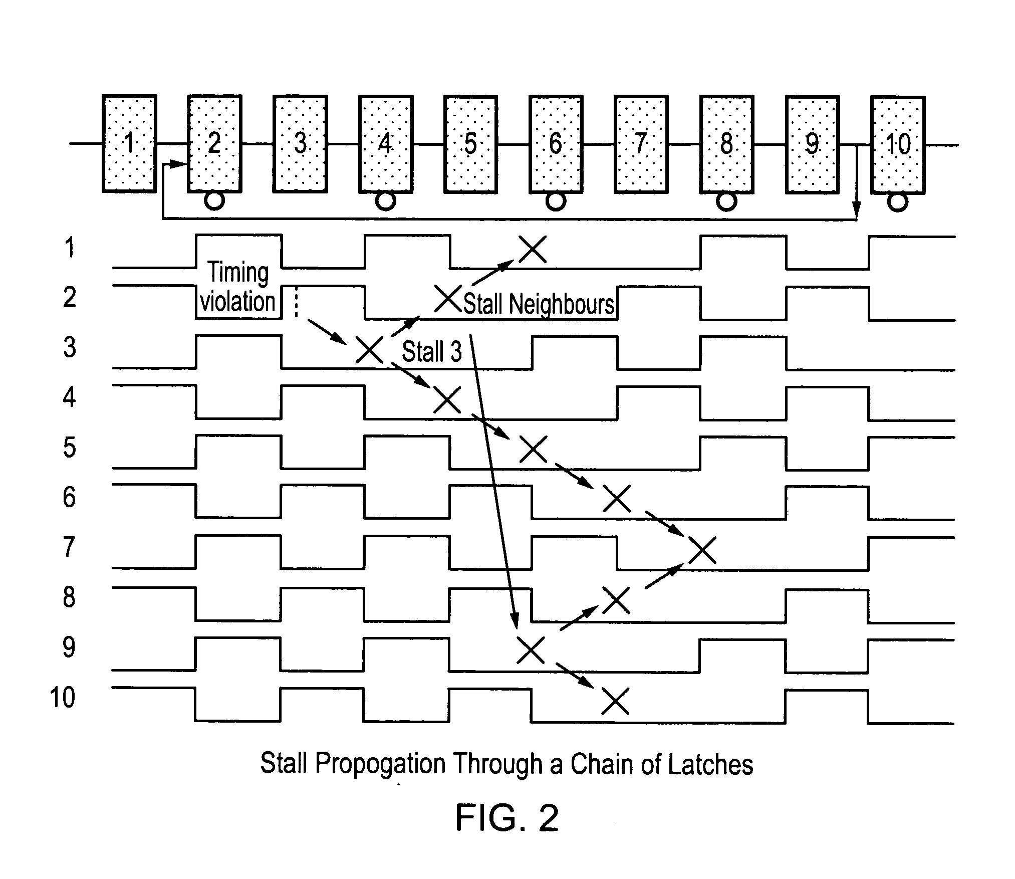
[0008]The present invention provides a system which provides the ability to detect instabilities on an input signal that occur within a predetermined time. In this way the system can detect cases where the data signal is not propagating through the system at the required rate, and is therefore changing during a period where it is expected to be stable. It deals with this error in an architecturally agnostic way by simply sending a control signal to initiate stalling of synchronisation circuits that receive the data. In this way, although the data may be changing late, synchronisation circuit(s) receiving it can be stalled for a cycle and this extra time allows for the data signal that was changing late to change within the required time.
[0047]Alternatively or additionally, the control circuitry can adjust the supply voltage at different locations and thus, if a certain portion of the circuit is providing more errors than another portion it can have its supply voltage increased. In this way, the circuit can be optimised to reduce error frequency without increasing power consumption by as much as would be the case if the whole circuit had its supply voltage increased.

Problems solved by technology

Furthermore, as the delay in the form of a stall, is propagated throughout the system along with the data, a stall of the whole system is provided without the need for a stall signal to be sent through the system in the same clock cycle, which is nearly impossible in a large system.

Method used


Image

  • Stalling synchronisation circuits in response to a late data signal
  • Stalling synchronisation circuits in response to a late data signal
  • Stalling synchronisation circuits in response to a late data signal

Examples


Embodiment Construction

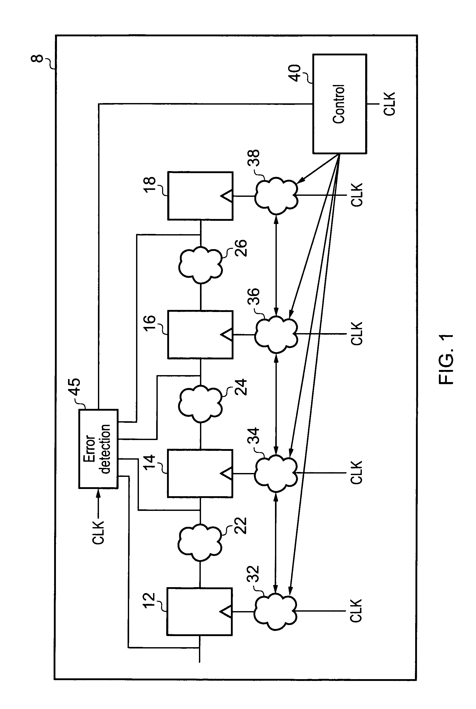
[0058]FIG. 1 schematically shows a portion of a data processing apparatus 5 according to an embodiment of the present invention. Data processing apparatus 5 has several synchronisation elements 12, 14, 16 and 18 which in this example are latches arranged in series with combinational logic 22, 24, 26 between them. These synchronisation circuits and combinational logic form a portion of a data path within data processing apparatus 5. Data is passed from synchronisation element 12 through synchronisation element 14, 16 and 18 in response to a clock signal and processing is performed upon the data by combinational logic 22, 24 and 26. Thus, as in this example the synchronisation elements 12, 14, 16 and 18 are latches, during a first phase of a clock cycle latch 12 is open and data is received at its input and as it is a transparent latch the data value is retained within the latch during this phase of the clock cycle and is present at its output. Combinational logic 22 therefore process...


PUM


Abstract

A data processing circuitry for processing data is disclosed. The data processing circuitry comprises: a plurality of synchronisation circuits for capturing and transmitting the data in response to a clock signal and a plurality of combinational circuits arranged between the synchronisation circuits for processing the data, the plurality of synchronisation circuits being arranged in at least two groups; an error detecting circuit for determining if the data input to one of the plurality of synchronisation circuits is stable during a predetermined time and for signalling an error if the data input is not stable, the predetermined time being less than a half cycle of the clock signal; control circuitry responsive to said error detecting circuit signalling said error to transmit a control signal to at least one of said groups of synchronisation circuits that contains a subsequent synchronisation circuit that said synchronisation circuit with said unstable input is configured to transmit said data to; each of said group of synchronisation circuits being configured to respond to receipt of said control signal to stall for a clock cycle and to transmit a stall signal to at least one further group of synchronisation circuits that said group of synchronisation circuits is configured to transmit data to or receive data from; each of said group of synchronisation circuits being configured to respond to receipt of said stall signal provided they have not stalled in a preceding clock cycle to stall for a clock cycle and to transmit a stall signal to said at least one further group of synchronisation circuits.

Description

BACKGROUND OF THE INVENTION[0001]1. Field of the Invention[0002]The field of the invention relates to the field of data processing and in particular to detecting and responding to errors.[0003]2. Description of the Prior Art[0004]Typical digital systems need to provide the correct output all of the time, and as these systems involve data being sampled at periodic intervals, ample time must be allowed for all combinational logic such that data will be ready under the worst operating conditions, most critical paths and most variable silicon. In order to account for these worst cases large margins are introduced which during normal operation are not needed and are a waste of power and performance.[0005]Another known way of addressing this problem is a razor-based system produced by ARM® Limited of Cambridge England. This is a system that is designed to operate at a point beyond this estimated absolute safe limit, the system having an error detection and recovery means to recover from c...

Claims


Application Information

Patent Timeline
Patent Type & Authority Applications(United States)
IPC IPC(8): G06F1/12
CPCG06F9/3869G06F11/0793G06F11/0721
Inventor FOJTIK, MATTHEW RUDOLPHSYLVESTER, DENNIS MICHAELBLAAUW, DAVID THEODOREFICK, DAVID ALAN
Owner RGT UNIV OF MICHIGAN
Learn More