Semiconductor device enabling refreshing of redundant memory cell instead of defective memory cell

a memory cell and memory cell technology, applied in the field of semiconductor devices, can solve the problems of large number of defective memory cells produced, difficulty in manufacturing all the memory cells without defects, and difficulty in handling the refresh operation

Active Publication Date: 2011-09-08
LONGITUDE LICENSING LTD
View PDF9 Cites 78 Cited by
  • Summary
  • Abstract
  • Description
  • Claims
  • Application Information

AI Technical Summary

Benefits of technology

[0013]In another embodiment, there is provided a semiconductor device that includes a first memory block and a second memory block that are selected according to a first address portion, wherein the first memory block and the second memory block are divided into a plurality of memory mats that each share the same bit line and are selected according to a second address portion, and the plurality of memory mats include a plurality of normal memory cells and a plurality of redundant memory cells that are selected according to a third address portion; and a redundancy determination circuit that, in response to an event in which at least one normal memory cell that is to be accessed is being replaced by a redundant memory cell in a case in which both the first memory block and the second memory block are accessed as a result of disabling the first address portion, inhibits the selection of a normal memory cell belonging to the same memory mat as a redundant memory cell that is to be replaced.

Problems solved by technology

Consequently, it is difficult to manufacture all the memory cells without any defects, and in practice a large number of defective memory cells are produced in the manufacturing stage.
In this case, how to handle the refresh operation when a refresh address is the address of a defective memory cell is a problem.
More specifically, at the time when a refresh operation is performed, for example, since the most significant bit of a row address is disabled, if an alternate access is merely performed in the same way as at the time when a normal operation is performed, even a word line without a defect will be regarded as the source of replacement, and thus the problem will arise in which word lines without a defect will no longer be selected at the time when a refresh operation is performed.
However, according to this method, since even defective word lines are activated although there is no need to activate them, there is the problem in which electric current consumption will increase at the time when a refresh operation is performed.
In that case, data is destroyed.
Thus, when simultaneously activating more word lines at the time when a refresh operation is performed than at the time when a normal operation is performed, there has been a problem with respect to the method of handling a replacement operation when a refresh address is the address of a defective memory cell or a defective word line.

Method used


Image

  • Semiconductor device enabling refreshing of redundant memory cell instead of defective memory cell
  • Semiconductor device enabling refreshing of redundant memory cell instead of defective memory cell
  • Semiconductor device enabling refreshing of redundant memory cell instead of defective memory cell

Examples


Embodiment Construction

[0024]The invention will now be described herein with reference to illustrative embodiments. Those skilled in the art will recognize that many alternative embodiments can be accomplished using the teachings of the present invention and that the invention is not limited to the embodiments illustrated for explanatory purposes.

[0025]An exemplary embodiment is described hereunder with reference to the attached drawings.

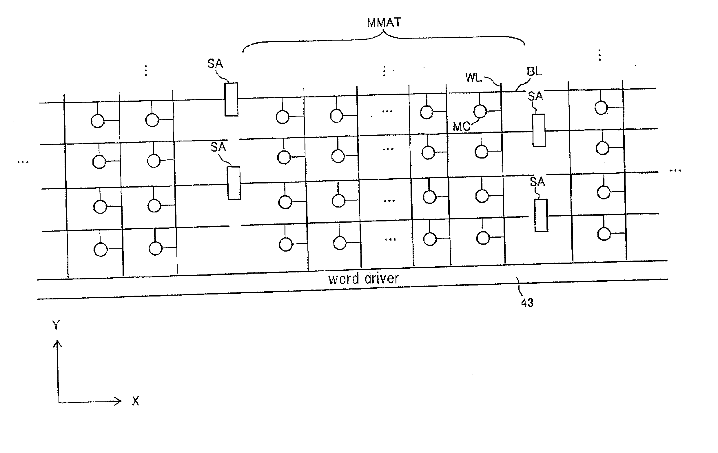
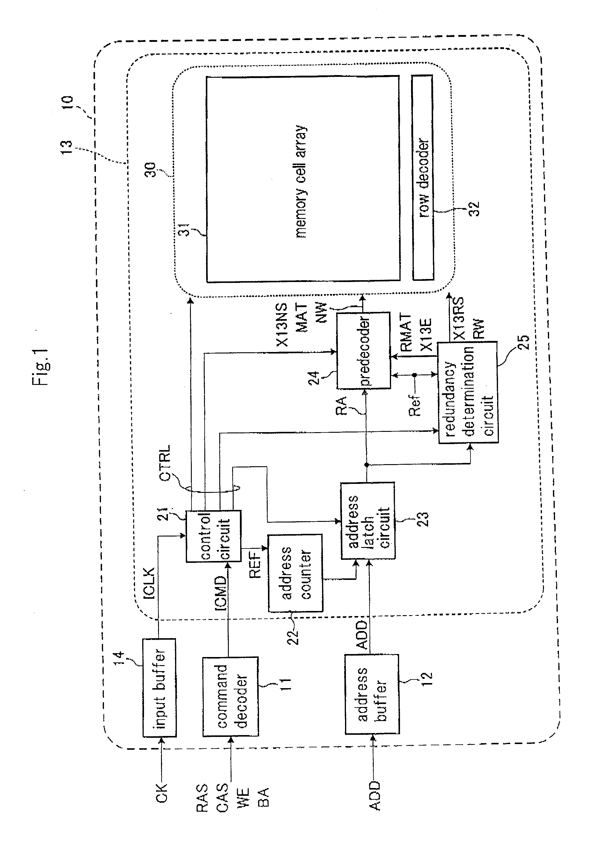
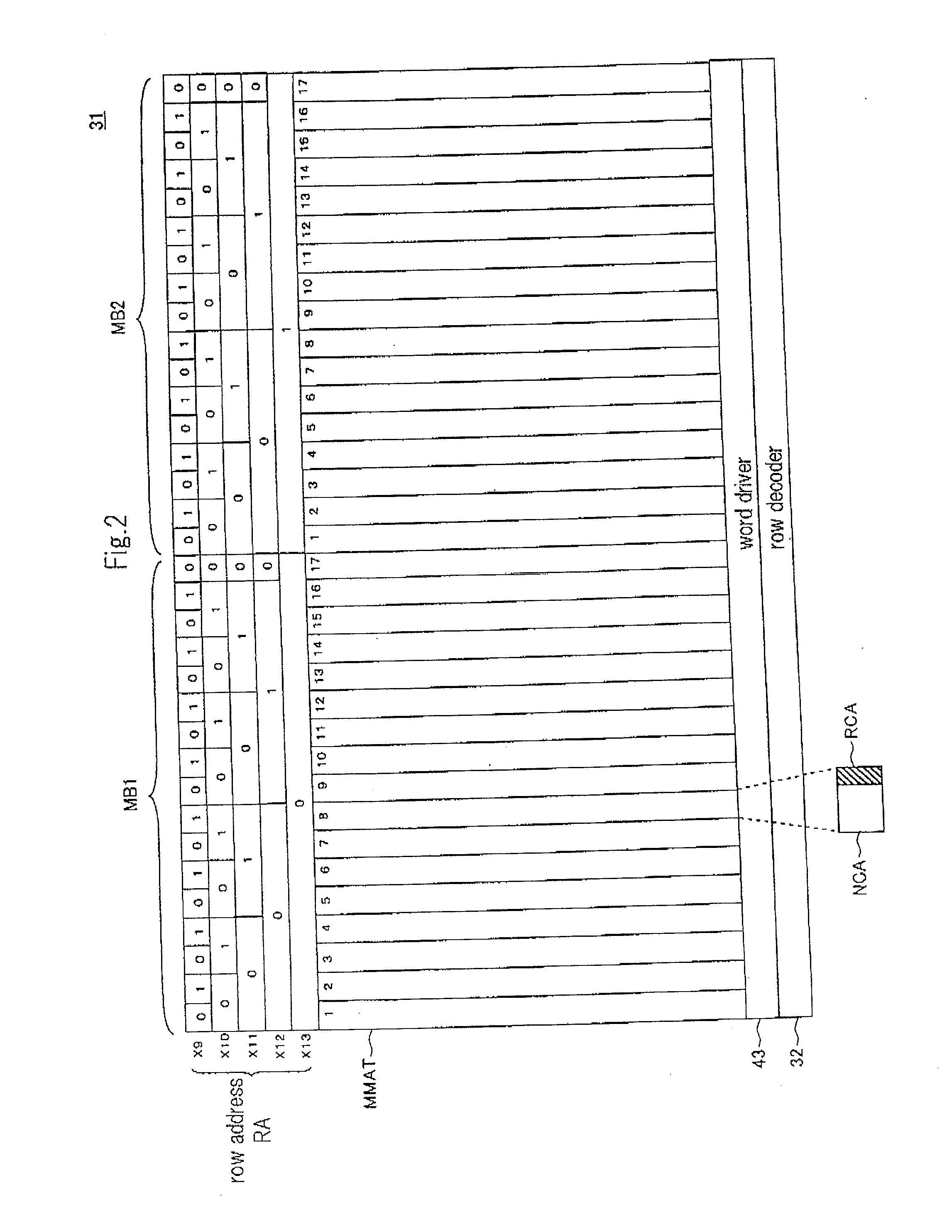
[0026]FIG. 1 is a block diagram that illustrates a configuration of a semiconductor device according to an exemplary embodiment.

[0027]As shown in FIG. 1, semiconductor device 10 according to the present exemplary embodiment is configured as a single semiconductor chip, and has command decoder 11, address buffer 12, and at least one memory bank 13 on the same chip. Memory bank 13 comprises control circuit 21, address counter 22, address latch circuit 23, predecoder 24, redundancy determination circuit 25, and memory area 30. Memory area 30 includes at least memory cell arr...


PUM


Abstract

A semiconductor device includes memory blocks MB1 and MB2 and redundancy determination circuit 25 that can enter a normal operation mode that accesses either memory block MB1 or memory block MB2 and a refresh mode that simultaneously accesses both memory block MB1 and memory block MB2. In response to normal memory cell NMC that belongs to at least one of memory blocks MB1 and MB2 being replaced by redundant memory cell RMC in the refresh mode, redundancy determination circuit 25 deactivates normal cell area NCA to which normal memory cell NMC that is a source of replacement belongs, and activates redundant cell area RCA to which redundant memory cell RMC that is to be replaced belongs and normal cell area NCA to which normal memory cell NMC that is not being replaced belongs.

Description

[0001]This application is based upon and claims the benefit of priority from Japanese Patent Application No. 2010-48818 filed on Mar. 5, 2010, the content of which is incorporated by reference.BACKGROUND OF THE INVENTION[0002]1. Field of the Invention[0003]The present invention relates to a semiconductor device that simultaneously activates more word lines during a refresh operation than during a normal operation.[0004]2. Description of Related Art[0005]The storage capacities of semiconductor memory devices as typified by a DRAM (Dynamic Random Access Memory) are increasing year by year, and accompanying such increases the area occupied by a single memory cell is being reduced more and more. Consequently, it is difficult to manufacture all the memory cells without any defects, and in practice a large number of defective memory cells are produced in the manufacturing stage. The addresses of defective memory cells are detected by an operation test that is conducted when semiconductor ...

Claims


Application Information

Patent Timeline
Patent Type & Authority Applications(United States)
IPC IPC(8): G11C29/04
CPCG11C29/04G11C29/08G11C11/406G11C29/783G11C29/808
Inventor HOSOE, YUKI
Owner LONGITUDE LICENSING LTD
Why Eureka
Try Eureka