
Plasma display panel and method for manufacturing the same

a plasma display panel and plasma technology, applied in the manufacture of electrode systems, electric discharge tubes/lamps, instruments, etc., can solve the problems of low productivity and high cost, difficult to form transparent electrodes with dimensional accuracy suitable for panels, and the patterning process above has limitations in dimensional accuracy and other issues, to achieve the effect of low cost, excellent image display, and small variations in discharge characteristics

Inactive Publication Date: 2011-09-15
PANASONIC CORP
View PDF3 Cites 0 Cited by
  • Summary
  • Abstract
  • Description
  • Claims
  • Application Information

AI Technical Summary

Benefits of technology

[0011]Such structured panel achieves low cost and small variations in discharge characteristics between discharge cells, providing excellent image display with high quality.

Problems solved by technology

Besides, the forming process above has a problem of low productivity and high cost.
A screen printing method and an inkjet method can be employed for applying dispersion liquid; however, the patterning by the aforementioned thick film printing has the limitations of dimensional accuracy.
Therefore, it has been difficult to form a transparent electrode having dimensional accuracy suitable for a panel.
Large variations in discharge gap due to poor dimensional accuracy of a transparent electrode increase variations in discharge characteristics between discharge cells.
This has brought mura to the display surface and impaired the quality of image display.

Method used


Image

  • Plasma display panel and method for manufacturing the same
  • Plasma display panel and method for manufacturing the same
  • Plasma display panel and method for manufacturing the same

Examples


Embodiment Construction

[0027]An exemplary embodiment of the present invention is described hereinafter with reference to the accompanying drawings.

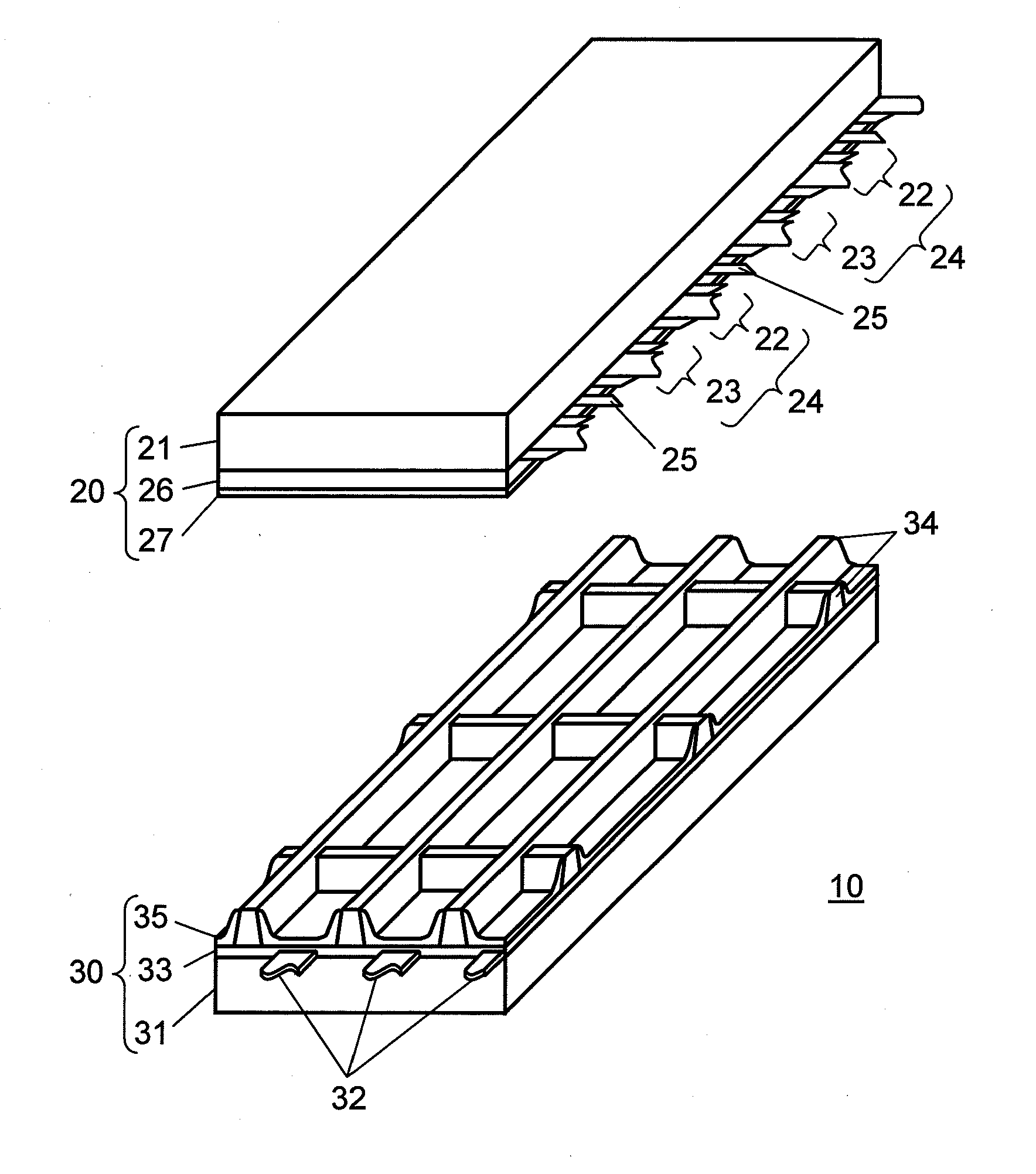
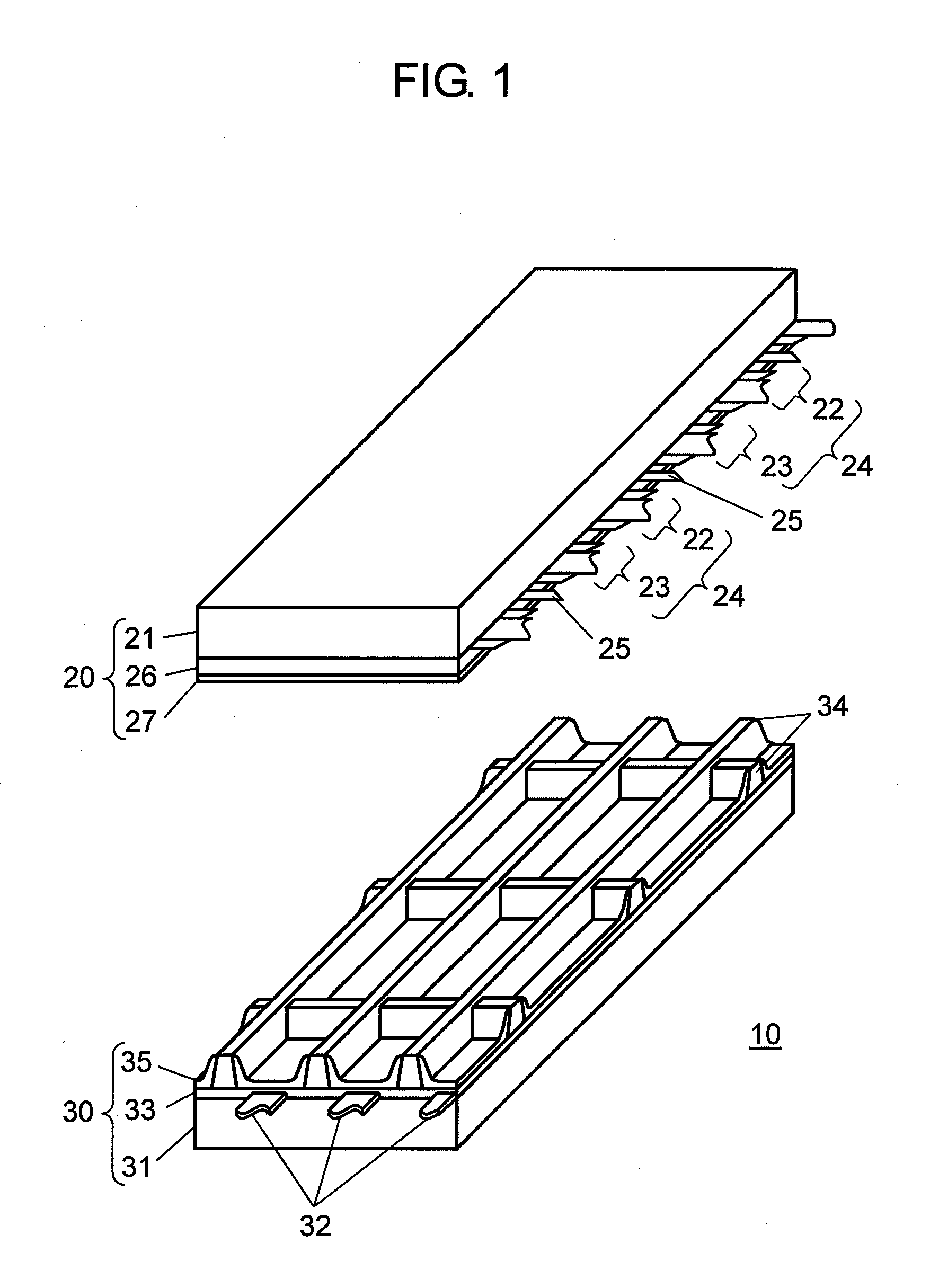
[0028]FIG. 1 is an exploded perspective view showing the structure of the panel in accordance with the exemplary embodiment of the present invention. Panel 10 has a structure where oppositely disposed front panel 20 and back panel 30 are sealed at the peripheries with sealing material (not shown) and a plurality of discharge cells are formed inside.

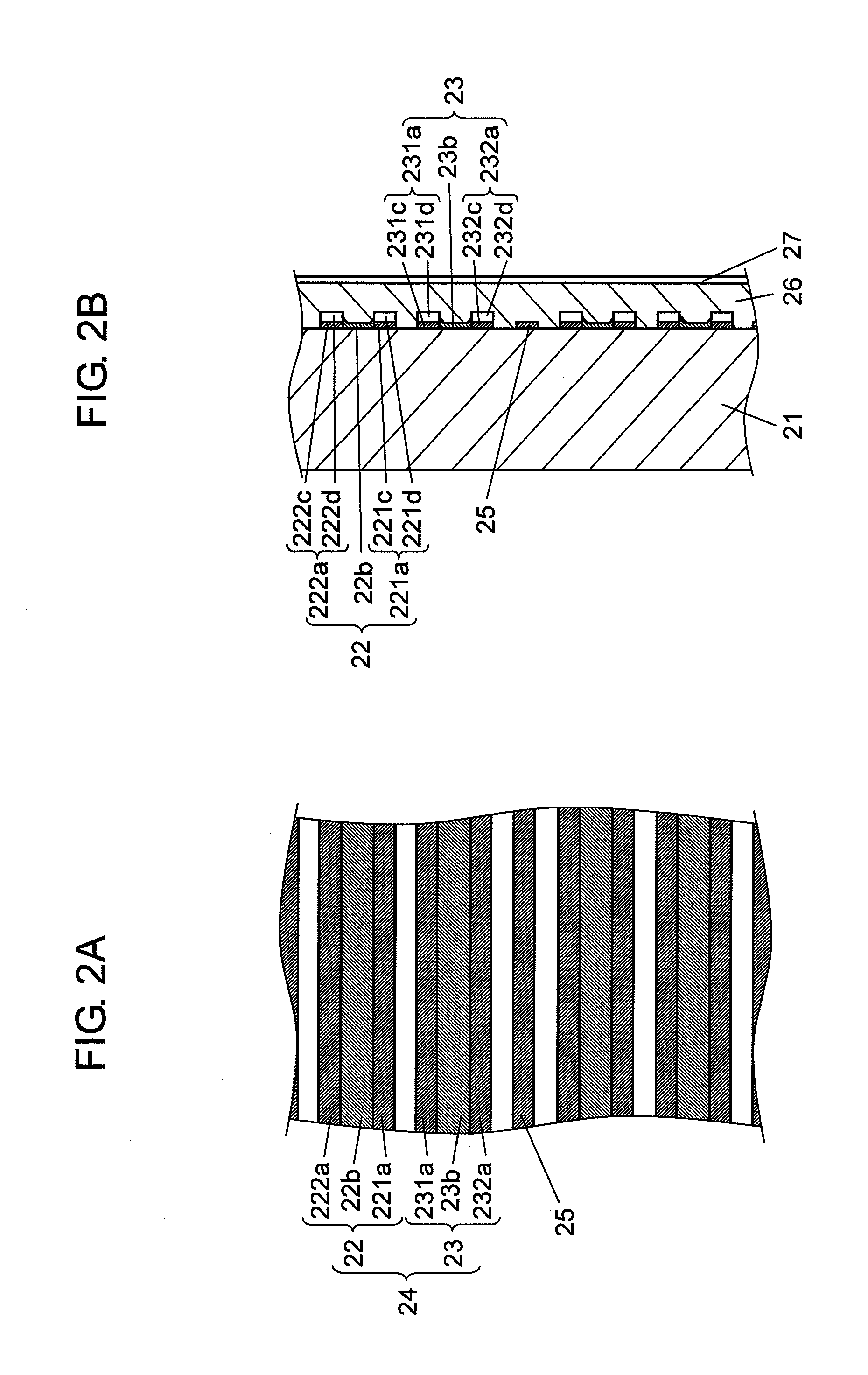
[0029]Front panel 20 has glass-made front substrate 21, display electrode pairs 24 formed of scan electrodes 22 and sustain electrodes 23, black stripes 25, dielectric layer 26, and protective layer 27. On front substrate 21, display electrode pairs 24, each of which is a pair of scan electrode 22 and sustain electrode 23, are formed in parallel with each other. Besides, black stripe 25 is formed between adjacent display electrode pairs 24.

[0030]Although FIG. 1 shows an arrangement of display electrode pairs 24 and b...


PUM

PropertyMeasurementUnit
thicknessaaaaaaaaaa
temperatureaaaaaaaaaa

Abstract

Having a low-cost transparent electrode, the plasma display panel suppresses variations in discharge characteristics between discharge cells and provides high quality image. To attain above, a scan bus electrode is formed so as to constitute an outer periphery in the lengthwise direction of a scan electrode and have a clearance inside, similarly, a sustain bus electrode is formed so as to constitute an outer periphery in the lengthwise direction of a sustain electrode and have a clearance inside. Besides, a scan transparent electrode is formed in the clearance of the scan bus electrode with use of a dispersion liquid containing particles of metal or particles of metal oxide, similarly, a sustain transparent electrode is formed in the clearance of the sustain bus electrode with use of a dispersion liquid containing particles of metal or particles of metal oxide.

Description

TECHNICAL FIELD[0001]The present invention relates to an AC surface discharge-type plasma display panel used for a display device and also relates to a method for manufacturing the panel.BACKGROUND ART[0002]An AC surface discharge-type plasma display panel, which has become dominance in plasma display panel (hereinafter simply referred to as a panel), has a front panel and a back panel oppositely disposed with each other and a plurality of discharge cells therebetween. The front panel has a glass front substrate, display electrode pairs each of which formed of a scan electrode and a sustain electrode, a dielectric layer and a protective layer that cover them. The back panel has a glass back substrate, data electrodes, a dielectric layer that covers the electrodes, barrier ribs, and phosphor layers. The front panel and the back panel are oppositely disposed and sealed with each other so that the display electrode pairs are located orthogonal to the data electrodes. The discharge spac...

Claims


Application Information

Patent Timeline
Patent Type & Authority Applications(United States)
IPC IPC(8): G09G3/28G06F3/038H01R43/00H01J9/02H01J11/22H01J11/24H01J11/34
CPCH01J9/02H01J11/12H01J11/24Y10T29/49117H01J2211/323H01J2211/444H01J11/32
Inventor ISHIKURA, YASUHISAURIU, EIICHIHAMADA, RYOTAMURAKOSO, TOMOHIRO
Owner PANASONIC CORP
Learn More