Method for fabricating semiconductor devices and a semiconductor device made therefrom

a semiconductor device and fabrication method technology, applied in semiconductor devices, semiconductor/solid-state device details, electrical devices, etc., can solve the problems of affecting affecting the efficiency of the laser lift-off process, and causing a residual stress that could damage the structure of the epitaxial layer stack, so as to achieve efficient and economical fabrication of semiconductor devices

Active Publication Date: 2011-09-22
NATIONAL CHUNG HSING UNIVERSITY
View PDF9 Cites 8 Cited by
  • Summary
  • Abstract
  • Description
  • Claims
  • Application Information

AI Technical Summary

Benefits of technology

[0008]Therefore, an object of the present invention is to provide a method for efficiently and economically fabricating semiconductor devices.

Problems solved by technology

However, the laser lift-off process involves a relatively high fabrication cost, whereas the mechanical thinning process involves the step of directly grinding and polishing off the temporary substrate.
The mechanical thinning process is likely to induce a residual stress that could damage the structure of the epitaxial layer stack.

Method used


Image

  • Method for fabricating semiconductor devices and a semiconductor device made therefrom
  • Method for fabricating semiconductor devices and a semiconductor device made therefrom
  • Method for fabricating semiconductor devices and a semiconductor device made therefrom

Examples


Embodiment Construction

[0034]Before the present invention is described in greater detail with reference to the accompanying preferred embodiments, it should be noted herein that like elements are denoted by the same reference numerals throughout the disclosure.

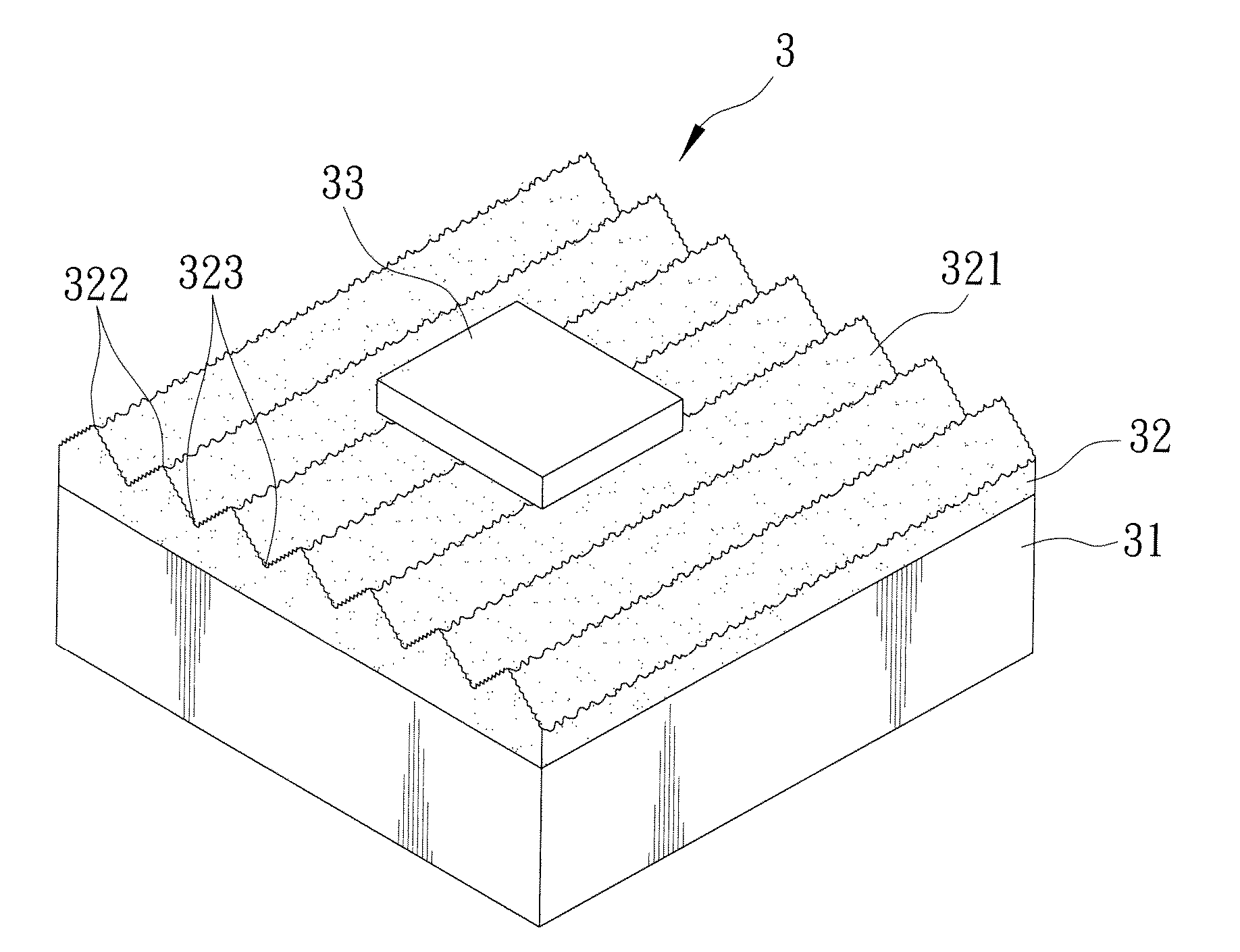
[0035]Referring to FIG. 3, the first preferred embodiment of a semiconductor device 3 according to the present invention includes a conductive member 31, an epitaxial structure 32, and an electrode 33.

[0036]The epitaxial structure 32 has a first side formed with a plurality of alternating protrusions 322 and indentations 323, and a rough surface 321 on the alternating protrusions 322 and indentations 323. Preferably, the protrusions 322 are configured as elongate strips that are substantially parallel to each other.

[0037]The conductive member 31 is formed on a second side of the epitaxial structure 32 opposite to the first side.

[0038]The electrode 33 is formed on the rough surface 321 of the epitaxial structure 32. By virtue of electrical connection...


PUM


Abstract

A method for fabricating semiconductor devices includes: (a) forming over a temporary substrate a sacrificial film layer; (b) growing laterally and epitaxially an epitaxial film layer; (c) forming over the epitaxial film layer a patterned mask that covers partially the epitaxial film layer and that defines a plurality of through holes to expose a plurality of epitaxial surface regions, respectively; (d) forming a plurality of conductive members respectively in the through holes and on the epitaxial surface regions; (e) removing the patterned mask and removing a part of the epitaxial film layer and a part of the sacrificial film layer beneath the patterned mask; (f) removing the sacrificial film layer; and (g) removing the temporary substrate.

Description

CROSS-REFERENCE TO RELATED APPLICATION[0001]This application claims priority of Taiwanese application no. 099107764, filed on Mar. 17, 2010.BACKGROUND OF THE INVENTION[0002]1. Field of the Invention[0003]This invention relates to a method for fabricating semiconductor devices and a semiconductor device made therefrom, more particularly to a method for fabricating semiconductor devices involving removing a temporary substrate without cutting a semiconductor structure formed thereon.[0004]2. Description of the Related Art[0005]Currently, there are various optoelectronic semiconductor devices on the market. Taking an example of a vertical-conducting light-emitting diode (LED), referring to FIG. 1, such optoelectronic semiconductor device 1 comprises a conductive member 11, an epitaxial structure 12 disposed on the conductive member 11, and an electrode 13 disposed on the epitaxial structure 12. By virtue of electrical connection with the conductive member 11 and the electrode 13, elect...

Claims


Application Information

Patent Timeline
Patent Type & Authority Applications(United States)
IPC IPC(8): H01L23/48H01L21/78
CPCH01L33/0079H01L33/405H01L33/22H01L33/20H01L33/0093
Inventor WUU, DONG-SINGHORNG, RAY-HUAWU, CHIA-CHENGYEN, CHENG-YING
Owner NATIONAL CHUNG HSING UNIVERSITY
Why Eureka
Try Eureka