Deformation-based micro surface texturing system
a texturing system and micro-surface technology, applied in the direction of dough shaping, manufacturing tools, instruments, etc., can solve the problems of high equipment cost, poor surface finish of products, and high cost, and achieve low cost, reduced energy consumption, and minimal material waste.
- Summary
- Abstract
- Description
- Claims
- Application Information
AI Technical Summary
Benefits of technology
Problems solved by technology
Method used
Image
Examples
example 1
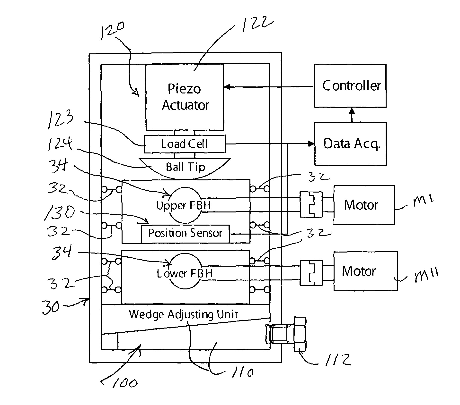
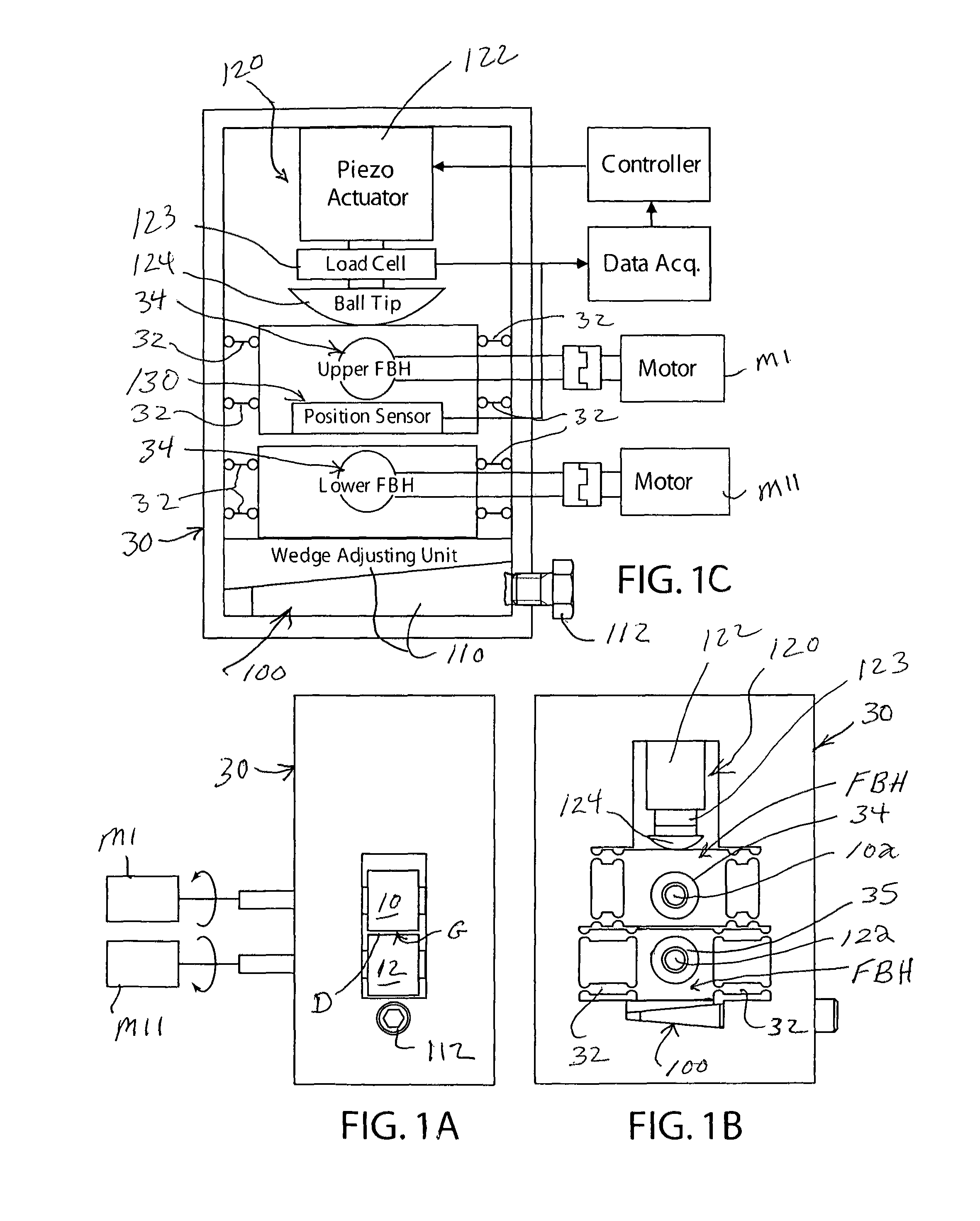
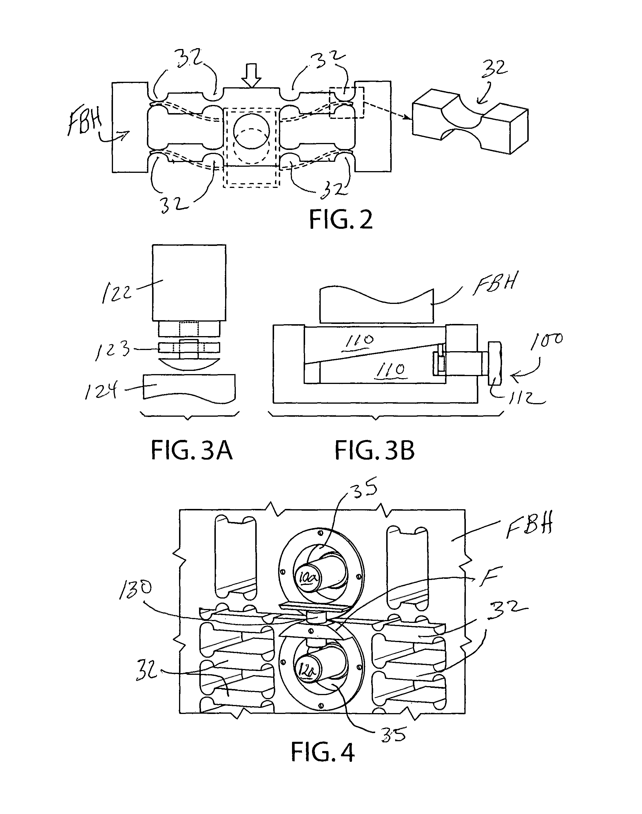
[0044]To validate the deformation-based surface texturing method of the invention, experiments were conducted using the apparatus described above with the main rigid housing or frame 30 with integral FBH's cut from one piece of high strength steel block using wire EDM to provide a rigid mono-block (monolithic) frame. The rigid frame 30 had an outer envelope having compact dimensions of 340 mm, 200 mm and 166 mm such that it could be placed on a desktop.
[0045]One surface of different AA5052 aluminum sheets (40 mm width and 100 mm length) were textured with micro channels to different depths. The roll gap between two rolls 10, 12 was adjusted to correspond to each required final depth of the micro channels. The rolls 10, 12 were 40 mm in length and 46 mm in diameter and were made of tungsten carbide. Piezoelectric actuators 122 were utilized to press the FBH's of the upper roll 10 to get nanometer accuracy of the roll gap dimension D. Signals from displacement sensors 130 were read by...
example 2
[0047]Other experiments were conducted using the apparatus of Example 1 to texture soft polymers including PP, Nylon, LDPE, and PMMA in sheet form having a thickness of 1 mm.
[0048]FIGS. 8A, 8B, 8C, and 8D are WLI images of the microsurface textures (microchannels) successfully formed on the various PP, Nylon, LDPE, and PMMA polymer sheets of Example 2. The mcirochannels had a width dimension of 100 μm and depth dimension of 25 μm.
Electrical-Assisted Micro Surface Texturing
[0049]The present invention further envisions another embodiment referred to as electrical-assisted surface texturing (designated EAST) useful, if needed, to texture certain hard metals, such as for example stainless steel and titanium, having high strength and large elastic recovery. EAST involves passing a continuous or pulsed electrical current (DC or AC) through the workpiece during micro deformation. Electrical-assisted forming can significantly improve the formability of the hard metal and reduce springback d...
example 3
[0052]Stainless steel strips with a width of 5 mm and thickness of 1.2 mm were used in the experiments to study the ESFT process. The rolling speed was 2 mm / s. Three cases of current densities through the contact area of the teeth of the upper roll and the sheet (strip) were studied, which were 15 A / mm2, 20 A / mm2 and 25 A / mm2. The required currents passed through the sheet were 90 A, 120 A and 150 A, respectively. With electrical current of 0 A, 90 A, 120 A and 150 A, the final depth of the micro channels are 34.5 μm, 38.5 μm, 44.6 μm, and 58 μm, respectively, FIG. 10. With 150 A current pass through, the depth of micro channel increased more than 68%.
[0053]Besides of increasing the depth of textured micro channels, the thickness of the sheet also reduced with electrical effect. For each case, five samples were textured, and the final thickness of the sample was measured. Without electrical current, the average final thickness of the sheet is 1.15 mm; while, with electrical current ...
PUM
| Property | Measurement | Unit |
|---|---|---|
| thickness | aaaaa | aaaaa |
| depth | aaaaa | aaaaa |
| depth | aaaaa | aaaaa |
Abstract
Description
Claims
Application Information


